Printed Circuit Board Panelization Basics
March 01, 2022
Blog
When you design a small run of boards for fabrication, it’s extremely likely that the PCB manufacturer will place it in a panel for manufacturing with a number of other designs. This “panelization” allows for boards to be made for low prices, since board space can be efficiently shared between orders.
When simply sharing space for efficient manufacturing, the process is largely transparent to the board designer. However, there are other instances where panelization must be given more thought. First of all, if a board is to be assembled by automated machinery, using a (still) panelized array of boards can speed up the process. It can also facilitate alignment via extra border space left on the perimeter of the array. It also makes automatic assembly of very small boards possible.
In other instances, it can be advantageous to obtain a board with snap-off sections. Perhaps there’s an A and B side of a design, or even a programming header that snaps off after a single use.
Panelize it Yourself?
If you’re allowing a single supplier to manufacture your board, and handle assembly as well, most likely they can handle panelization for you. In fact, there’s a good chance–as seen around the 12:00 mark in this video by PCB manufacturer Royal Circuits–that they’d prefer this method anyway. However, if you’re running the assembly operation yourself, you may have specific wants or needs for how a panel is put together, and you’ll want to specify things manually.
Kyle Hunter, at MicroType Engineering, shows off his panelization process using KiCad in the this video. Here he’s using mouse bite tabs, where small tabs are designed to snap off for board separation. Some things may have changed since the video was made (2020), but he gives a good overview of the concepts involved, including some discussion about border thickness versus potential warping issues.
A second panelization technique is called v-scoring, where boards are cut partway through the PCB. This technique is generally used with PCBs that have straight edges, and as shown here, this, as well as mouse bites, are fairly simple to set up using the EasyEDA online design package and JLCPCB as the supplier. Depending on your PCB manufacturer, and EDA software you’ll likely want to get in touch with your board supplier directly to make sure everything is in order if using v-scoring.
Panelization in KiCad
While I’ve personally never ordered a self-panelized board, I did design one some time ago with the idea that I could fold it into a box. This arrangement turned out to be very expensive if I remember correctly, and eventually “folded” it into a project and article focused on castellated holes.

Caption: Potentially inappropriate panelization usage
Image Credit: screencap Jeremy Cook
If you do want to manually specify mouse bite tabs, this can be done in KiCad, and this video gives specifics on how to do so manually. It even includes downloadable footprints in the video description. One challenge may be aligning the footprints properly with your grid. If needed, use shift + m to move things into alignment. This technique is not perfect, and making revisions would be tedious, but it’s there if you need it.

Image Credit: https://github.com/yaqwsx/KiKit
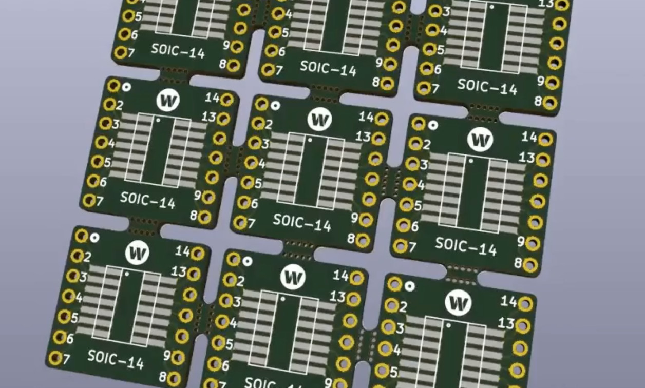
Another interesting option here is the KiKit automation plugin, which takes care of panelization, as well as other tasks. Unfortunately, installation on MacOS (i.e. my computer) can be problematic, and I haven’t actually tried it out beyond an unsuccessful install. For other systems it looks well worth an install, and perhaps on Mac as well if you’re willing to do a bit more yak shaving.
Depanelization: The Finished Product
If a PCB is panelized, it must also be de-panelized. Snapping panels off of each other is rather simple, it still adds a step to your process. Depending on your manufacturer, and whether you go with mouse bites or v-scores, you may also be left with artifacts that need to be cleaned up. Dealing with one or two boards isn’t generally a big deal, but if you’re doing this to hundreds, or even thousands of boards, it’s worth asking the question of what your finished product will look like!
Image Credit: screencap: https://www.youtube.com/watch?v=lJU9Zu-mMXw
Jeremy Cook is a freelance tech journalist and engineering consultant with over 10 years of factory automation experience. An avid maker and experimenter, you can follow him on Twitter, or see his electromechanical exploits on the Jeremy Cook YouTube Channel!