How to Design Castellated PCBs for Board-to-Board Attachment
September 24, 2021
Blog
Castellated holes on a PCB, also known as castellations or crenellations, are plated through holes on a PCB which are cut in half. Typically, these are applied to the outer edges of a board, and are used to solder one board on top of another.

Test castellations installed in a more conventional role. Surface mount pads work well, but through holes were problematic. (Image Credit: Jeremy Cook)
Why Castellations?
This ability to attach one board on top of another as a module allows for a number of different design options that wouldn’t be available otherwise.

XIAO SAMD21 breakout with dual castellated/through hole pads (Image Credit: Jeremy Cook).
Consider, for example, if you’re designing a board and would like to integrate wireless capabilities. Rather than designing everything yourself, it may be much easier to buy a module to take care of the wireless features, such as an ESP-12F. With the proper pad spacing, castellated PCB modules can be soldered on, simplifying design and certification requirements.
While not a wireless device, I wrote about the XIAO SAMD21 device here, which features castellations on its edges, combined with more traditional through holes on its connection pads. This design is also shared with the Raspberry Pi Pico. At the cost of a slightly larger board, this type of dual-hole setup gives these and similar devices a huge amount of connection flexibility.
In addition to pre-built modules, there may be a situation where most of a board can be made with only one or two layers, while a certain segment of the design requires a more expensive multi-layer process. The ability to attach an extra board allows for much more design flexibility, potentially saving production costs. In a related–and certainly less conventional–usage, I was also able to implement castellations in a cube-shaped LED PCB arrangement. This is perhaps more artistic than functional, and isn't’ exactly easy to troubleshoot.
Integrate Castellations into Your Design?
If you’d like to use castellated holes in your design, the good news is that it’s extremely easy. In fact, in VoltLog’s castellation video below, he actually explains how to do this using KiCad in roughly 5 seconds at the 4:10 mark: “Use through hole pads and run the board outline through the middle of those.”
There is a trick, however, which comes when you’re ordering PCBs, and/or your expectations for when you get them back. In my case, I ordered PCBs from PCBWay, which allows you to indicate that there are castellations on your design, tacking on $16 to the PCB price. Supplier OSHPark does not charge for castellations, however they don’t claim full support for them either. Practically speaking, what this means for OSHPark is that, while potentially less expensive, you may have to clean up the castellated board when you get it back.
According to the VoltLog video, you can also leave the castellated holes box unchecked with PCBWay for potential cost savings + extra burrs. I have yet to try it, though perhaps it could save you a few bucks if you’re willing to deal with cleaning things up.
Experimental Cube Light Design


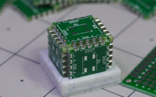
Cubic PCB “flower” and 3D-printed jig used for assembly (Image Credit: Jeremy Cook).
For this article, I decided I needed to actually make some castellated boards, and came up with a quick design for PCBs that were castellated. My unconventional design is a cube that can be soldered together in three dimensions. It mounts input and output connectors for wires, as well as 5 addressable LEDs.
Perhaps it wasn’t the easiest design for my first castellated PCB(s), but it seems to have worked out after a bit of rather tedious connection troubleshooting. Design-wise, there were a few challenges, in part because the circuit was split out into two distinct boards. Perhaps I’ll talk about it more in a future post.

Image Credit: Jeremy Cook
Actual routing can be a bit touchy when trying to start traces, as it doesn’t appreciate them starting inside a board outline. Generally you can start traces internally, but you also may need to edit a pad’s properties with the e key to move one in ever-so-slightly to connect. This KiCad footprints post may be instructive here as well.
More Info
If you’d like a bit more info on how PCBs are manufactured, I found this video interesting and instructive:
For lots more background on using castellated modules, Altium Academy put out the excellent video seen below:
Interestingly, towards the end of the clip, presenter Ben Jordan notes that a very popular use for castellations is for solder-on IoT wireless modules. Unfortunately, while using such a device helps with RF testing requirements, they don’t actually eliminate them. However, more info on EMI compliance testing when using a module can be found here.
Jeremy Cook is a freelance tech journalist and engineering consultant with over 10 years of factory automation experience. An avid maker and experimenter, you can follow him on Twitter, or see his electromechanical exploits on the Jeremy Cook YouTube Channel!