Reuse and Design Custom KiCad Footprints
August 13, 2021
Blog
In a previous post, I outlined how you can manage and customize new symbols in KiCad, allowing you to accurately depict your circuit designs.
To take your design from “paper” into the real world of printed circuit boards (PCBs) you’ll need to assign symbols to footprints that show components’ physical sizes, allowing you to arrange them and the corresponding connections as needed. Here I’ll go over finding or designing new footprints for KiCad, and integrating them into your design.
Try to Find (Before You Design)

Image Credit: Jeremy Cook
If you don’t have a component footprint available, the first thing you’ll want to do is a quick web search to see what’s available for download. No reason to repeat someone else’s work if you don’t have to. In a recent project I used keyswitch footprints found here, along with the layout for a Sparkfun Pro Micro (AKA Arduino Pro Micro) that I downloaded from this repository to complete the design.
A few minutes of poking around can save you a lot of time, and potentially give you a better footprint model than you’d be likely to come up with for personal use. Once you have it downloaded, place the footprint library folder in a known location, perhaps in a lib_fp.pretty directory as described in this best practices article if you’re going to use it on a particular project. You might also choose a central location if you plan to use it in a variety of projects.

Image Credit: Jeremy Cook
In Pcbnew, the main KiCad menu, or Footprint Editor, open up Pereferences > Manage Footprint Libraries…. Select either the Global Libraries or Project Specific Libraries tab depending on if you want to us a library everywhere or just on one particular project, then hit the folder icon to add your downloaded library to the selected table.
Inside library folders, there will be .kicad_mod files, which correspond to individual footprints. With your new footprints properly set up, you can assign them to symbols in a particular design through the Layout Editor, or via the symbol editor via the Library Symbol Properties interface to tie them to a particular symbol.
Your Very Own Footprint

Image Credit: Jeremy Cook
If and when you’ve failed to find an acceptable footprint on the good ol’ World Wide Web, it’s time to break out your datasheet and/or calipers. Open the footprint editor–the IC icon in the main KiCad screen–and select File > New Library. Save your newly named library in a convenient place–again, perhaps under an overall lib_fp.pretty directory. This will create a new .pretty directory in which you can store new footprints. You can also modify an existing library with new footprints, but best to keep those pristine for the time being.
Click on the chip icon with this new library selected to create an actual footprint, where you’ll be asked for a name for your new part, then be presented with an interface that looks strikingly similar to the PCB Layout Editor. Essential elements here include the Add pad icon to place the pads for your component, as well as geometric drawing tools for the component’s courtyard and silk screen.

Caption: Not a particularly useful component
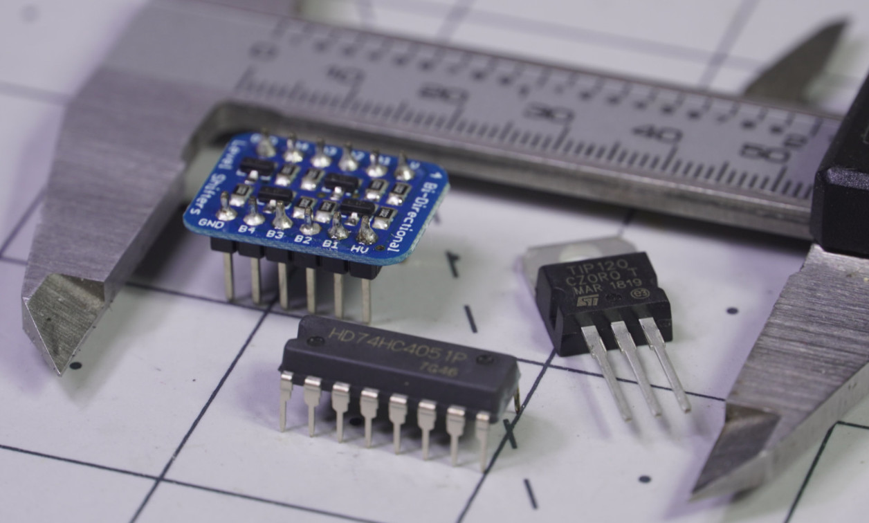
Image Credit: Jeremy Cook
Measure your parts or analyze the datasheet, better yet both, then duplicate the component’s footprint on KiCad based on this data. You’ll want to make sure the pad numbers are consistent with the datasheet, and that your pad spacing is correct to avoid any connection issues.
For more info on how components can be represented, you can open parts in existing libraries, and hit the e (edit) key on different elements to see how it be modified. I’d just avoid saving anything until you’re sure you want to make changes. The Schematix video above also gives a nice overview of how to create your own footprints, as well as schematic symbols if you would like an overview of the process.

Caption: Not my footprint, but interesting for examination
Image Credit: Jeremy Cook
The ability to add or make custom footprints opens up a number of new possibilities, allowing you to take KiCad PCB designs much further than would otherwise be possible. While largely optional–though certainly helpful to avoid mechanical clearance issues–you can even associate 3D models with your 3D footprints.