GreenPAK AC-Power Cycle Skip Control with System Monitoring
March 09, 2021
Story
Most home-based electrical appliances generally use AC power for operation. Cycle skip logic can be used in appliances such as AC dimmers, heaters, and cookers.
These electrical appliances consist of power electronic switches like Silicon Controlled Rectifier (SCR)s, and Triode for Alternating Current (TRIAC)s which are turned ON/OFF periodically to achieve smooth operation.
In this control, the load is turned ON for a set number of cycles and is turned OFF for a set number of cycles. Figure 1 displays the cycle skip logic output. As evidenced from Figure 1, the load is turned ON for a cycle and turned OFF for one cycle. The load is completely turned OFF due to the property of TRIACs which is described in detail in Section 3. This control scheme also reduces EMI as no excessive dI/dt is present.
Channel 1 (blue/top line) - AC Supply
Channel 2 (green/bottom line) - Cycle Skip Output

Figure 1: Cycle Skip Output
This article is divided into 3 sections. Section 1 describes a zero-crossing circuit, Section 2 illustrates the generation of different patterns including system monitoring features using GreenPAK, and section 3 defines a TRIAC driver circuit for driving the load.

Figure 2: Opto-isolator with Phototransistor
1. Zero Crossing Circuit
A zero-crossing circuit consists of an AC power supply, a half-wave rectifier, and an opto-isolator with a photo-sensitive device - phototransistor. The opto-isolators isolate AC and DC signals using light. This opto-isolator consists of a LED, a light beam, and phototransistor as shown in Figure 2. The half-wave rectifier rectifies the input HIGH voltage AC signal and feeds the rectified output to the input LED of the opto-isolator. The signal from the LED then converts to an intensity proportional to the input signal and falls on to the base of the phototransistor which in turn triggers the phototransistor to the ON state. The output of the phototransistor is a DC signal which is used for generating different patterns in GreenPAK. Figure 3 displays the zero crossing circuit waveforms.
Channel 1(blue/top line) - AC Supply
Channel 2 (green/2nd line) - Half Wave Rectifier Output
Channel 3 (yellow/bottom line) - Opto-Isolator Output

Figure 3: Zero-Crossing Circuit Waveforms
2. GreenPAK Design
Figure 4 reveals the GreenPAK Design for generating different patterns for driving the load along with system monitoring features. This design can be used worldwide as it supports both 50Hz and 60Hz AC frequencies. This design includes both controls ( i.e. hardware and software). It was created in the GreenPAK Designer software and the complete design file can be found here.
The phototransistor output of the zero-crossing circuit arrives at Heater_Zero (Pin 2). Both edges of the input signal are then internally debounced for 2.5ms to ensure proper zero crossing edge detection. Subsection 2.1 describes the hardware control, Subsection 2.2 describes the software control, and Subsection 2.3 describes the system monitoring features. After the patterns are generated through the control mechanisms, they are then routed and displayed on the Heater_Enable (Pin7). This Heater_Enable (Pin 7) is then connected to the TRIAC driving circuit for driving the load.

Figure 4: GreenPAK Design
2.1 Hardware Control
The hardware control technique requires an external active LOW push-button which is connected to Push_Button #1 (Pin 5). If the button is pressed for a period less than 50ms, Heater_Enable (Pin 7) goes LOW, and when the button is pressed for a period greater than 50ms, the programmed patterns are displayed on Heater_Enable (Pin 7).
4 8-bit patterns with power levels of 0%, 25%, 75%, and 100% are designed on-chip, and 2 power levels - 25% (3-bit LUT3) and 75% (3-bit LUT5) are user selectable. Each button press executes an 8-bit pattern (programmed on-chip) generated through DFF chain and displays the patterns on Heater_Enable (Pin 7) only if the system monitoring features are in range. On the fifth button press, the patterns cycle through.
This control includes 2 system monitoring features - Over Temperature Protection (OTP) and Emergency Shutdown.
Figure 5 displays hardware control waveforms. As seen from Figure 5, zero-crossed AC signal arrives at Heater_Enable (Pin 2) and at each button press (Push Button #1 (Pin 5)) a pattern is displayed on the Heater_Enable (Pin 7). The Heater_Enable (Pin 7) is held LOW when the button is pressed for a period less than 50ms or when the system monitoring features are out of range.
2.2 Software Control
The software control requires an external I2C compatible MCU. In this control, a pattern in the range of 1-bit up to 16-bits is written on the programmable Pattern Generator (PGEN) via I2C.
Channel 1 (yellow/top line) – PIN#9 (Input Voltage)
Channel 2 (blue/2nd line) – PIN#11 (Temperature Monitor)
D0 – PIN#6 (Push Button #2)
D1 – PIN#5 (Push Button #1)
D2 – PIN#2 (Heater_Zero)
D3 – PIN#7 (Heater_Enable)

Figure 5: Hardware Control Waveforms

Figure 6: PGEN Timing Diagram
The data is displayed on PGEN's output at every rising edge of the clock when it's nReset terminal is held HIGH and when nReset is LOW, the first bit (D0) is displayed on its output. Figure 6 displays the timing diagram of PGEN block. In this design, 16 bits are written on the PGEN block and data repeats after 16-bits as long as the nRESET terminal is held HIGH. The pattern is displayed on Heater_Enable (Pin 7) as long as all the system monitoring features - Emergency Shutdown, OTP, and Watchdog Timer are in range.
Figure 7 displays software control waveforms. As evidenced from Figure 7, the pattern is only displayed on Heater_Enable (Pin 7) at every rising edge of Heater_Zero (Pin 2), when Software Enable is HIGH and all system monitoring features are in range.
Channel 1 (yellow/top line) – PIN#9 (Input Voltage)
Channel 2 (blue/2nd line) – PIN#11 (Temperature Monitor)
D0 – I2C OUT0 (Software Enable)
D1 – I2C OUT1 (Watchdog Timer In)
D2 – PIN#6 (Push Button #2)
D3 – PIN#2 (Heater_Zero)
D4 – PIN#7 (Heater_Enable)
D5 – PIN#12 (Watchdog Timer)

Figure 7: Software Control Waveforms

Figure 8: OTP Schematic
2.3 System Monitoring Features
OTP, Emergency Shutdown, Watchdog Timer, and Frequency Detection are the system monitoring features included in this design.
2.3.1 Over Temperature Protection
OTP feature is available in both hardware and software control techniques. This feature requires an external resistor divider with a thermistor. A thermistor is a temperature dependent resistor, whose resistance decreases with increase in temperature.
Figure 8 shows the OTP schematic. The sensed voltage is connected to Input Voltage (PIN 9). The temperature range inside GreenPAK is accomplished with a set of 2 Analog Comparators (ACMPs) and a LUT. In this design, the operational temperature range is set from 0˚C to 60˚C, which respectively corresponds to a voltage range from 2.176V to 0.928V for ACMPs. When the temperature is out of range the system is OFF, and when the temperature is in range, the design functions according to the chosen user control, i.e. hardware or software.
Figure 9 displays the OTP waveforms. As seen from Figure 9, the temperature monitor output is HIGH only when the temperature is in range, and the output is LOW when the temperature is out of range.
Channel 1 (yellow/top line) – PIN# 9 (Input Voltage)
Channel 2 (blue/bottom line) – PIN# 11 (Temperature Monitor)

Figure 9: OTP Waveforms
2.3.2. Emergency Shutdown
Emergency shutdown has the highest priority and this feature is available for both hardware and software control techniques. This feature is accomplished with an external active LOW push button which is connected to Push Button #2 (Pin 6) input on the IC. When the button is pressed the
Channel 1 (yellow/top line) – PIN# 6 (Push Button #2)
Channel 2 (blue/bottom line) – PIN# 2 (Heater_Zero)
D0 – PIN# 7 (Heater_Enable)

Figure 10: Emergency Shutdown
Heater_Enable (Pin 7) output goes LOW and the system turns OFF. When the button is released, the system turns back ON, depending upon software or hardware control and if other system monitoring features are in range. Figure 10 displays the emergency shutdown feature. As observed from Figure 10, when the button is pressed, the output at Heater_Enable (Pin 7) is disabled.
2.3.3. Watchdog Timer
This feature is available in software control only and is controlled through an I2C compatible MCU. CNT3 (8-bit) sets period of the watchdog timer. At POR, CNT3 is loaded with a value determined by
Channel 1 (yellow/top line) – I2C Virtual Input 1 - OUT1 (Watchdog Timer In)
Channel 2 (blue/bottom line) – (CNT3 Output)
D0 – PIN# 12(Watchdog Timer)

Figure 11: Watchdog Timer
Channel 1 (yellow/top line) – PIN# 2 (Heater_Zero)
Channel 2 (blue/bottom line) – PIN# 10 (Frequency Detect)

Figure 12: Frequency Detector
its control data register, which is 656.25ms (default). The timer operates continuously through a toggled I2C Virtual Input 1 - OUT1. If the MCU freezes or the I2C Virtual Input 1 - OUT1 is not toggled before 656.25ms, then the timer expires after 656.25ms and produces a 3ms reset pulse at watchdog timer (Pin 12). If the timer expires, then Heater_Enable (Pin 7) is LOW and the system turns OFF. Both timer period and reset pulse duration are user selectable and can be changed through I2C.
Figure 11 displays watchdog timer waveforms. As indicated in Figure 11, when I2C Virtual Input 1 - OUT1 is toggled before 656.25ms, the watchdog timer output is LOW and indicates the timer is in range, and when the I2C Virtual Input 1 - OUT1 is toggled at a time larger than the set CNT period, then the timer expires after 656.25ms (default) and the watchdog timer output turns HIGH.
2.3.4. Frequency Detector
CNT2 is used to detect the frequency of the input signal. The frequency detect output is HIGH when consecutive edges of the input signal arrive before the set counter period, and frequency detect output is LOW when consecutive edges arrive later than the counter period.
Figure 12 displays the frequency detector output. As seen from Figure 12, the frequency detect output is LOW when the input signal frequency is 50Hz, and the output is HIGH when the input signal frequency is 60Hz.
2.4 Modifying the Pattern Generator
For specific power consumption, different patterns are written on PGEN macrocell via I2C. To re-write different patterns, the following steps are recommended.
1. Assert Software_Enable (I2C Virtual Input 0 - OUT0) LOW
2. Write a new 16-bit pattern on PGEN registers
3. Assert Software_Enable HIGH
Following these steps in sequence guarantees proper synchronization of the new data written on PGEN registers. Table 1 shows the I2C address of the PGEN macrocell.
Table 1: PGEN I2C Address

3. TRIAC Driver Circuit
The TRIAC driver circuit consists of an opto-isolator with photo-TRIAC, and TRIAC for driving the load.
Figure 13 shows the opto-isolator with photo-TRIAC. As seen from Figure 13, the opto-isolator is comprised of a LED, a zero-crossing detector circuit and a photo-sensitive device, photo-TRIAC. This isolator isolates DC and AC signals. The patterns generated from the GreenPAK device are connected to the input LED of the opto-isolator. The zero-crossing detector circuit precisely detects true zero crossing of each AC signal.
The outputs of the opto-isolator are connected to the power TRIAC, which is then connected to the load. A positive pulse at the gate of the TRIAC triggers it to the ON state. The property of a TRIAC is that it automatically turns OFF at each half cycle of the sinusoidal supply voltage as the instantaneous voltage and load current falls to zero. The TRIAC starts latching the data once again at the next half cycle. The TRIAC can be turned OFF by either reducing the current across its terminals below its minimum holding current, or when the supply voltage is cut-off. The signal at the power TRIAC is the desired cycle skip output of the input AC signal.

Figure 13: Photo-TRIAC Opto-isolator
4. Testing
Figure 14 depicts the schematic of the cycle skip logic using GreenPAK. The main components of the test setup are a half-wave rectifier, an opto-isolator with phototransistor, a GreenPAK IC, an opto-isolator with photo-TRIAC, and a TRIAC. The test schematic shows the opto-isolators used for testing. The base of the phototransistor is connected to GND to achieve a stable output and reduce false triggering due to electrical noise.
As shown in Figure 14, the input AC signal is applied across LIVE and Neutral terminals and the output load is connected across Load_LIVE and Load_Neutral terminals. There are two external buttons, each connected to Push Button #1 (Pin 5) and Push Button #2 (Pin 6). The voltage across the resistor divider is connected to Input Voltage (Pin 9). An I2C compatible MCU is also present for the software control of the design. MCU's SCL and SDA lines are respectively connected to GreenPAK's SCL and SDA lines through pull-up resistors.

Figure 14: Cycle Skip Test Schematic
Figure 15 displays software control cycle skip outputs of the test schematic with the assumption that all the system monitoring features are in range. Data on PGEN macrocell is written through I2C by following the steps in Subsection 2.4. After 16-bits, on the 17th edge the pattern repeats as long as the software enable is HIGH. Once the software enable goes LOW, the cycle skip output also goes LOW.
Channel 1 (magenta/top line) - (AC Input)
Channel 2 (yellow/2nd line) - PIN#2 (Heater_Zero)
Channel 3 (black/3rd line) - I2C Virtual Input 0 - OUT0 (Software Enable)
Channel 4 (blue/4th line) - PIN#7 (Heater_Enable)
Channel 5 (green/bottom line) - Cycle Skip Output

Figure 15: Software Control Cycle Skip Output
Channel 1 (magenta/top line) - (AC Input)
Channel 2 (yellow/2nd line) - PIN#2 (Heater_Zero)
Channel 3 (black/3rd line) - PIN#5 (Push Button #1)
Channel 4 (blue/4th line) - PIN#7 (Heater_Enable)
Channel 5 (green/bottom line) - Cycle Skip Output

Figure 16: Hardware Control Cycle Skip Output
Figure 16 shows hardware control cycle skip outputs with the assumption that all system monitoring features are in range. At each button press, a pre-programmed power level is routed to Heater_Enable (Pin 7) and appropriately displayed on the cycle skip output. The programmed power levels each are 8-bit patterns. On the 9th bit, the pattern repeats if the button is still pressed. Once the button is released, Heater_Enable (Pin 7) goes LOW and also the cycle skip output. At the 5th button press, the pre-programmed power levels cycle through.
5. Feature Extension
The GreenPAK IC can be configured with any MCU capable of communicating through I2C. The DA14531 SmartBond TINY™ Development Kit-USB consists of IOs which can be configured as open drain outputs for I2C communication.

Figure 17: DA14531 USB Development Kit based Test Schematic
6. Demonstration PCB

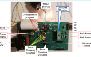
Figure 18: Cycle Skip and Phase Cut Control PCB
Figure 17 displays the test setup of cycle skip control using the DA14531 USB Development Kit. As shown in Figure 17, P0_2 (Port 0 - Pin 2) and P0_8 (Port 0 - Pin 8) pins are respectively configured as SCL and SDA for I2C communication. The power to DA14531 USB Development Kit is provided through a USB port in the kit. Please follow the steps in Subsection 2.4 to send I2C commands to GreenPAK's PGEN macrocell for modifying the patterns. Similar results of the cycle skip outputs are obtained when I2C commands are supplied through DA14531 USB Development Kit.
Figure 18 shows the demonstration board for both cycle skip and phase cut logic. This PCB can be readily used worldwide as the GreenPAK design supports both 50Hz and 60Hz AC frequencies. The user needs to only connect the AC mains supply and load. AC mains supply is applied to the board through the AC mains connector. For this demonstration, a light bulb is used as a load.
As shown in Figure 18, 2 separate TRIAC drivers and configuration jumpers are present on the board to switch from cycle skip to phase cut logic. The design is programmed on the GreenPAK DIP socket and 2 push buttons are present for hardware control of the designs and emergency shutdown respectively.
Test points for both connecting a 5V DC supply and communicating to the GreenPAK DIP socket through an I2C (SCL and SDA) compatible MCU are present on top right corner of the PCB.
This board also supports a DA14531 based Microbus socket to control GreenPAK through I2C communication.
Conclusion
The GreenPAK design described in this article is easy to use, minimizes cost, saves board space and component count. Generally, MCUs have limited IOs. So, offloading the control to small and inexpensive ICs saves IOs for other scritical operation.
Moreover, these ICs are flexible and easy to test. The design can be modified to include additional system monitoring features, increase/decrease pattern length as well as the number of patterns (hardware control only). This flexibility saves time and can accommodate last minute design changes. Once the design is modified, a new design file can be programmed on-chip with a click of a few buttons, and then re-soldered onto the board. It also offers design security by locking the design file to limit the visibility. By using this design, the user can control 4 8-bit patterns by push button, and 16-bit pattern through I2C.

Experienced professional in designing and implementing digital, analog, and mixed-signal circuits; simulation, troubleshooting, and bench validation.