How to Use LTspice to Produce Bode Plots for LED Drivers
August 16, 2021
Blog
Proper control loop phase and gain measurements should be made by factory experts possessing (expensive) equipment and commensurate experience. For those who do not have access to one or either of these, there is an alternative.
Closed-loop gain and phase plots are well-worn tools used to determine the stability of the control loop in switching regulators. Gain and phase measurements, when done properly, require access to, and familiarity with, fancy network analyzers. The measurements involve breaking the control loop, injecting noise, and measuring the resulting gain and phase over a frequency sweep (see Figure 1). This practice of measuring the control loop is rarely applied to LED drivers.
LED driver control loop phase and gain measurements require a different approach (see Figure 1)—a deviation from the typical resistive-divider-path-to-GND voltage regulator injection and measurement point. In both cases, benchtop control loop phase and gain measurements are the best way to guarantee stability, but not every engineer has at their fingertips the required equipment and access to an experienced factory apps team. What do these engineers do?
One option is to build the LED driver and see how it responds to transients. Transient response observation requires the application board and more common benchtop equipment. The results of transient analysis lack the Bode plot’s frequency-based gain and phase numbers—which can be used to guarantee stability—but they can act as a telltale for general control loop stability and speed.
Large signal transients can be used to check absolute deviation and system response time. The shape of the transient disturbance indicates the phase or gain margin and thus can be used to understand general loop stability. For instance, a critically damped response might indicate 45° to 60° phase margin. Or, a large spike during the transient can indicate the need for more COUT or a faster loop. A long settling time can indicate the need to speed up the bandwidth (and crossover frequency) of the loop. These relatively easy system checks enable on-the-fly characterization of a switching regulator’s control loop, but gain and phase Bode plots are required for deeper analysis.
LTspice simulation can be used to generate both switching regulator output transients and Bode plots before circuits are assembled or fabricated. This can help to get a rough idea of control loop stability—a starting point for compensation component choices and output capacitor sizing. The process of using LTspice based on Middlebrook’s original recommendation in 1975 is well documented (see “LTspice: Basic Steps in Generating a Bode Plot of SMPS”).1 The actual signal injection location laid out in Middlebrook’s method is not commonly used these days but has been adjusted over the years, resulting in the commonly used injection location shown in Figure 1a.
Furthermore, LED drivers, with high-side sense resistors and complicated AC resistance LED loads, should have a different injection point than either today’s injection point or Middlebrook’s original recommendation in the feedback path, one not previously demonstrated in LTspice. The method presented here shows how to generate LED driver current-sense feedback loop Bode plots in LTspice, and in the lab.
Producing Control Loop Bode Plots
Standard switching regulator control loop Bode plots yield three critical measurements, which can be used to determine stability and speed:
- Phase margin
- Crossover frequency (bandwidth)
- Gain margin
It is generally accepted that 45° to 60° of phase margin is required for a stable system, and that –10 dB gain margin is required for guaranteed loop stability. The crossover frequency relates to general loop speed. Figure 1 shows the setup for making these measurements using a network analyzer.
LTspice simulation can be used to create a similar injection and measurement in the control loop for an LED. Figure 2 shows an LED driver (LT3950) with an ideal sine wave of given frequency (f) injected directly into the feedback path on the negative sense line (ISN). Measurement points A, B, and C are used to calculate the gain (dB) and the phase (°) at the injection frequency (f). In order to graph the entire control loop Bode plot, this measurement must be repeated over a large frequency sweep, stopping at fSW/2 (half of the switching frequency of the converter).

Figure 1. Switching regulator control loop Bode plot measurement with a network analyzer for (a) voltage regulator and (b) LED driver. To make the measurement, the control loop is broken and a sinusoidal perturbation pushes into a high impedance path, while the resulting control loop gain and phase is measured, enabling the designer to quantify the stability of the loop.

Figure 2. LT3950 DC2788A demonstration circuit LED driver LTspice model with control loop noise injection and measurement points.
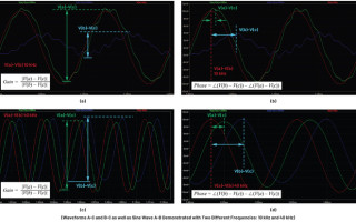
The measurement of points A, B, and C in Figure 2 determine the gain and phase of the control loop at the injection frequency (f). Different injection frequencies yield different gain and phase. For simplicity, and to see how this works, one can set the injection frequency and measure the gain and phase of A-C and B-C. This yields a single frequency point of the control loop Bode plot. Figures 3a and 3b show the gain and phase of 10 kHz ±10 mV AC injection. Figures 3c and 3d show the gain and phase of 40 kHz ±10 mV AC injection.
A sweep of frequencies and the measurements of gain and phase between B-C and A-C are what form the entire closed-loop Bode plot. As mentioned in the Abstract, this is typically accomplished on the bench using a fancy (that is, expensive) network analyzer. Such a sweep is also possible in LTspice, as shown in Figure 4. These results are confirmed by comparing them to the results of a benchtop test using a network analyzer (see Figure 8).

Figure 3. The measurement of points A, B, and C in Figure 2 determine the gain and phase of the control loop at the injection frequency (f). Different injection frequencies yield different gain and phase. Figures 3a and 3b show the gain and phase of 10 kHz ±10 mV AC injection. Figures 3c and 3d show the gain and phase of 40 kHz ±10 mV AC injection. A sweep of frequencies and the measurements of gain and phase between B-C and A-C are what form the closed-loop Bode plot.

Figure 4. Bode plot measurements with the LT3950 in LTspice showing gain (solid line) and phase (dashed line).
Make Full Gain and Phase Sweeps and Plots in LTspice
To create a full Bode plot, a graphical sweep of gain and phase, in LTspice for the control loop, follow these steps.
Step 1: Create the AC Injection Source
In LTspice, insert the ±10 mV AC injection voltage source and injection resistor and label nodes A, B, and C as shown in Figure 2. The AC voltage source value SINE(0 10m {Freq}) sets the 10 mV peak and sweeps the frequency. The user can play with peak sine values between 1 mV and 20 mV. Keep in mind that sense voltage for many LED drivers is 250 mV and 100 mV. Higher injection noise can create LED current regulation errors.
Step 2: Add the Math
Insert the .measure statements on the schematic as .sp (SPICE) directives. These directives perform Fourier transforms and compute the complex open-loop gain and phase of the LED driver in dB and phase.
Here are the directives:
- .measure Aavg avg V(a)-V(c)
- .measure Bavg avg V(b)-V(c)
- .measure Are avg (V(a)-V(c)-Aavg)*cos(360*time*Freq)
- .measure Aim avg -(V(a)-V(c)-Aavg)*sin(360*time*Freq)
- .measure Bre avg (V(b)-V(c)-Bavg)*cos(360*time*Freq)
- .measure Bim avg -(V(b)-V(c)-Bavg)*sin(360*time*Freq)
- .measure GainMag param 20*log10(hypot(Are,Aim) / hypot(Bre,Bim))
- .measure GainPhi param mod(atan2(Aim, Are) - atan2(Bim, Bre)+180,360)-180
Step 3: Set the Measurement Parameters
A few more small directives are needed. First, the circuit must be in a steady state of the simulation (past startup) in order to make proper measurements. Adjust the t0, or start time for the measurement, and stop time. The start time can be estimated or garnered by starting up the simulation and observing the start-up time. The stop time is chosen to be 10/freq, or 10 periods, after steady state is reached—reducing errors by averaging over 10 cycles for each frequency.
Here are the directives:
- .param t0=0.2m
- .tran 0 {t0+10/freq} {t0} startup
- .step oct param freq 1K 1M 3
Step 4: Set the Frequency Sample Step and Range
The .step command sets the frequency resolution and range over which to perform the analysis. In this example, the simulation runs from 1 kHz to 1 MHz using a resolution of three points per octave. Bode plot measurements are accurate up to fSW/2, so the upper frequency limit should be set to half of the switching frequency of the system. Obviously, more points improve resolution, but the simulation takes longer. Three points per octave is the low end of resolution, but running the simulation at minimum resolution can save some time. Nevertheless, looking at the overall design cycle picture, a 5-minute simulation is orders of magnitude faster than designing, assembling, and testing PCBs. With this in mind, you may want to just run at a higher resolution, such as five or more points per octave, to produce more complete and easier to view results.
Step 5: Run the Simulation
It seems straightforward, but LTspice requires multiple production steps to produce the Bode plot. The first step is Run the Simulation, which does not yield (yet) the plot, but instead shows normal scope voltage and current measurements. Follow the next steps to produce the Bode plots.
Step 6: Produce the Bode Plot
Open the SPICE Error Log by right-clicking the schematic window and choosing Plot .step’ed .meas data. Choose Visible Traces from the Plot Settings Menu and select Gain to plot the data. Optionally, measurement data can be exported by clicking File and selecting Export Data as Text to produce a CSV file of the Bode data.
Bode Plot Confirmation with a Network Analyzer—Beyond Simulation
Simulation of control loops is not as reliable as the real thing and should not be used for a complete guarantee of loop stability and margins. At some stage of the design process, the control loop should be verified in the lab using a network analyzer tool.
The Bode plots generated in LTspice can be compared to network analyzer Bode plot measurement results. Just like the simulation, the actual loop measurements are captured by injecting noise into the feedback loop and measuring and processing the A-B and A-C gain and phase. The measurement setup schematic and photo are shown in Figure 5 through Figure 7.

Figure 5. LED driver control loop Bode plot measurement setup using a network analyzer.

Figure 6. Venable System Model 5060A vintage network analyzer used for high-side floating noise injection and measurement of LED drivers.

Figure 7. Noise injection and measurement points on the LT3950 LED driver.

Figure 8. Bode plots for the LT3950 LED driver on a DC2788A demonstration circuit. The plots generated through LTspice simulation (blue line) have a strong correlation to those generated using a network analyzer (green line).
Table 1. Bode Plot Measurement Data Comparison of LTspice vs. Network Analyzer for the LT3950 LED Driver
|
Test Setup |
Crossover Frequency (kHz) |
Gain Margin (dB) |
Phase Margin (°) |
|
Network analyzer, 8 VIN |
16.75 |
17.47 |
83.96 |
|
LTspice, 8 VIN |
15.8 |
13.79 |
71.23 |
|
Network analyzer, 12 VIN |
30.41 |
18.71 |
83.73 |
|
LTspice, 12 VIN |
47.36 |
5.04 |
62.29 |
LTspice simulation results show a strong correlation to network analyzer data, proving that LTspice is a useful tool in LED driver design—producing a rough baseline to aid the engineer in narrowing the range of component choices. The gain and phase at lower frequencies closely follow hardware, with a greater difference between simulation and hardware data at higher frequencies. This might represent the challenge of modeling high frequency poles, zeroes, parasitic inductances, capacitances, and equivalent series resistances.
Conclusion
LTspice modeling can be used to measure control loop gain and phase, thus producing Bode plots for LED drivers. The accuracy of the LTspice simulation data is dependent on the accuracy of the SPICE models used, though carefully modeling each component to account for real-world behavior comes at the cost of increased simulation times. For the purpose of LED driver design, LTspice data is useful for relatively quickly narrowing the field of components and predicting general circuit behavior even without perfect component modeling. A working simulation helps guide the design engineer before transitioning to hardware implementation, saving overall design time. Once rough component choices have been made, measurements using a built board with a network analyzer can confirm or contrast the simulation results as a means of hardware validation during development.
Reference:
1. Gabino Alonso. “LTspice: Basic Steps in Generating a Bode Plot of SMPS.” Analog Devices, Inc.
Keith Szolusha is an applications director with Analog Devices in Santa Clara, California. Keith has worked in the BBI Power Products Group since 2000, focusing on boost, buck-boost, and LED driver products, while also managing the power products EMI chamber. He received his B.S.E.E. in 1997 and M.S.E.E. in 1998 from MIT in Cambridge, Massachusetts, with a concentration in technical writing. He can be reached at [email protected].
Brandon Nghe is an applications engineer at Analog Devices. He received his M.S.E.E. from California Polytechnic State University in 2020. Brandon is responsible for the design and testing of boost, buck-boost, and LED driver DC-to-DC converters for low EMI automotive applications. He can be reached at [email protected].

Keith Szolusha is an applications director with Analog Devices in Santa Clara, California. Keith works in the BBI Power Products Group, which focuses on boost, buck-boost, and LED driver products, while also managing the power products EMI chamber line. He received his B.S.E.E. in 1997 and M.S.E.E. in 1998 from MIT in Cambridge, Massachusetts, with a concentration in technical writing.
Brandon Nghe is an applications engineer at Analog Devices. He received his M.S.E.E. from California Polytechnic State University in 2020. Brandon is responsible for the design and testing of boost, buck-boost, and LED driver DC-to-DC converters for low EMI automotive applications.