System-on-Chip (SoC) Design- and Development Considerations ? Part 2
March 27, 2019
Story

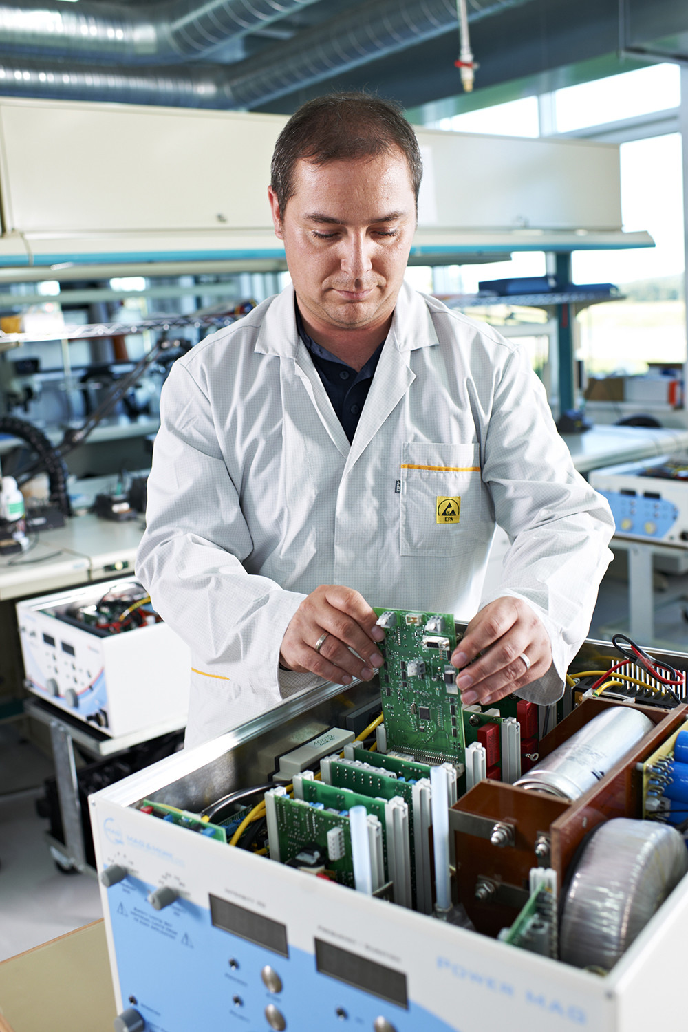
Design of a control module based on the Arria 10 SoC for use in a medical application.
The optimal methodology leads to success
The prerequisite for large FPGA designs generally consists of close cooperation and an intensive exchange of information between customers, developers, PCB manufacturers, board manufacturing and FPGA manufacturers. For the implementation of these tasks, HEITEC has defined a methodology that places great emphasis on clear definitions, comprehensive documentation and ongoing reviews, especially in the early stage of the projects. The concept must be specified from scratch and the required functionalities and architecture must be clearly defined so that the development process can proceed efficiently and without large re-designs. It is especially important to document each phase of the project in detail. The preliminary discussions with the customer are the basis for a requirement-based design. The goal is a requirements specification, i.e. by drawing up a requirements table including functions and performance parameters, as well as the electrical, mechanical and thermal properties. The next steps are concept specification, function specification, development and implementation as well as verification and validation of functions using system simulation.
Concept specification
One of the first steps is the concept specification, which defines all requirements, the implementation concept, the FPGA selection and the data transfer model. This can extend over weeks or even months for highly complex projects and results in a detailed document with sometimes over 100 pages of description, high-level block images and tables. In this phase, the functional partitioning is determined, i.e. the definition of which functions are realized in hardware or software as well as which hardware components (CPU, FPGA, ASIC, SoC) are used. For different solutions, a decision matrix is created to select the essential components such as CPU, SoC, High Speed I/O interfaces, memory interfaces, etc.
Here, too, it is determined which IPs will be used. For example, it may be necessary to integrate a processor for control and debugging tasks into the FPGA, as at high speeds conventional measurements on the chip are sometimes no longer possible and by means of appropriate software and pattern generators internal self-tests must be performed. The corresponding status registers, error counters, error bits, etc. can be used to determine whether the desired functionality has been achieved and to be able to correct faults step by step. During the concept phase, the system performance and real-time capability as well as the electrical, mechanical and thermal properties are also being assessed. Especially important at this stage is the timing and cost estimate for the overall project, including specification, FPGA and board development, software development and commissioning, up to prototypes and then, if necessary, from the prototype to the product, ready for series production.
Functionality specification
The functional specification defines both hardware and firmware design specifications. The specification of the hardware design concerns the FPGA as well as all the essential components on the board. It includes defining the FPGA architecture, selecting and describing the FPGA components, estimating the power and voltage requirements for the board and FPGA, detailed function block diagrams, module descriptions, flow charts, mapping the FPGA I/O Pins, the clock and reset concept, the hardware and software interfaces and the required test environment.
As a result of the firmware design specification, detailed flow charts, the selection of the operating system, boot concept, and definition of low-level driver and test routines are available. Also, it specifies interaction tests, application details, firmware/software interfaces, diagnostic support and error handling.
Quality assurance
With the start of the actual design, it is of paramount importance to take further comprehensive measures for quality assurance. Close reviews are the appropriate method for this, as this already identifies many errors in the specification and in the code. This may seem cumbersome, but it is very effective and increases quality at an early stage. The exchange of experience between developers via reviews and inspections automatically implies an increase of development know-how in the various phases of the project. These measures are complemented by extensive checklists and consistent version management. High-level design entry tools such as Mentor HDL Designer are used for the implementation, and the verification and validation of the functions are done by a FPGA module-/system simulation that spans fully automated self-checking test benches with BFMs, scoreboards, assertions, regression, etc.
Proven concepts of ASIC design
Crucial to successful ASICs development is that the design’s overall functionality is fully verified before the data is handed over to the ASIC manufacturer. Malfunctions in the final design are very difficult and, above all, expensive to fix due to the elaborate production of masks. In contrast, FPGAs feature greater flexibility in fixing design flaws and implementing functional changes. However, in order to be able to meet the given usually tight schedule and cost framework for highly complex FPGA designs, the design methodology, as it is described here, is essential.
This is the only way to avoid retrospective and usually only intricately implementable functional changes as well as lengthy and expensive fault analyses. Moreover, high-speed aspects can be strictly considered in the concept, the FPGA architecture, the I/O pinning and the VHDL coding from the very beginning of the early design phases. Good coding guidelines as well as skillful pipelining and registering pay off later during synthesis and P & R.
Therefore, HEITEC developers also consistently use their many years of experience in ASIC design for the design of high-speed FPGA solutions.
Initially, the development team analyzed the system specifications. In systems with an Arria 10, the FPGA typically plays a big role in the overall system and affects the rest of the system design. It is important to illustrate the design process as transparently as possible by creating detailed design specifications for the system and FPGA, and by defining the FPGA input and output interfaces to the rest of the system.
Intensive data processing includes several send and receive paths, where large amounts of data processing can lead to high dynamics for the numerical outputs. The more send and receive paths are designated, the higher, of course, the requirements. Hard floating point functionality is very helpful for this, provides increased stability and is much more powerful at 1.5 GHz than previous technologies.
With the hard floating point DSP blocks in the Arria 10, FPGA systems are able to overcome many of the performance-limiting challenges and to dramatically reduce power consumption. The architecture eliminates 100 percent of the IEEE 754 floating point logic normally implemented with FPGA resources. First, all necessary requirements are recorded in the hardened DSP blocks. This eliminates the need to create denormalization and normalization logic with valuable FPGA resources. In the past, hardware implementation was not immediately possible. Often, the algorithm had to be converted in several steps into a fixed point implementation optimal for FPGA architectures. The simplified implementation eliminated elaborate debugging and significantly reduced development time.
Various considerations played a special role during the design process: Specifying the I/O interface for the FPGA, identifying the different clock domains, defining a block diagram of the basic design functions, integrating IP blocks, elaborating a verification/test plan of functions for the entire team (Design for Manufacturability). In addition, a general design directory structure was beneficial as it facilitated the different levels of integration. The target of this concept was the FPGA programming via JTAG port and loading the updates of the FPGA configuration as well as the HPS CPU software via GUI-PC Ethernet interface.
This blog is Part 2 of a 3-part series. Click here for Part 1 and Part 3.
Roland Chochoiek
Executive VP Electronics HEITEC AG
Roland holds degrees in Electronics and Business Administration and worked in a number of senior management positions within the high-tech industry, including Force Computers, Solectron and Rittal. Since 2010 he has been the Executive Vice President of the Electronics Business Unit of HEITEC AG.