Why Your Embedded ADC Does not Perform to the Data Sheet and How to Improve its Performance, Part 2: Clock and Reference Selection
September 25, 2018
Story

In this installment, we will share additional details to help you select the right clock and the right reference for the application.
In part 1 of this series, we presented the reasons why an embedded analog-to-digital converter (ADC) performance in the data sheet might not represent your application. These reasons included characterization of the ADC while the rest of the system of chip (SoC) was quiet, consideration of the entire signal chain instead of just the ADC in isolation (because operational amplifiers can degrade the signal, reducing the ADC output converted), and some topics of configuration that impact performance. In this installment, we will share additional details to help you select the right clock and the right reference for the application.
Clock selection
Clock jitter impacts the signal-to-noise ratio (SNR) of an ADC for non-DC signals. A higher SNR means there is more signal and less noise (resulting in better performance). Clock jitter results in a skew in sample time. If that skew is small compared to the sample rate, then it doesn’t impact performance much. But the higher the input signal frequency, the more jitter reduces the SNR. Equation 1 shows the relationship to calculate the maximum jitter for the desired ADC performance (SNR):

Figure 1 graphically shows this impact, with some example numbers.
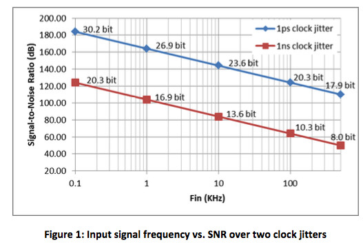
Ideally, the data sheet would list the jitter for each clock source, but that is seldom the case – or the data sheet does not provide all of the information you need to calculate the jitter of interest. The lowest jitter performance is always found in the external crystal, but that comes at an increased cost if you don’t need the crystal for other parts of the system. An external crystal also requires additional power and a longer startup time (which decreases the power saved by duty cycling the ADC and its contributing IP, which can include the clock and reference). Table 1 summarizes typical clock-source options and the benefits and costs associated with each option. For a deeper dive on clock jitter refer to reference [1] and [2].
|
Clock source
|
Jitter
|
Cost
|
Suggested use
|
|
EXT CLK
|
Lowest
|
Requires an external crystal
Higher power
Longer to start up
|
When you need the best performance at higher-input signal frequencies
|
|
INT PLL
|
Medium
|
Needs an external crystal for lower jitter
Higher current
Longer to start up
|
If the phase-locked loop (PLL) is already on when using the ADC and doesn’t require the lower jitter gained by using an external crystal
|
|
INT OSC
|
Highest
|
No external components
Can have fast startup
|
Best for lower-frequency input signals
|
Voltage references
There are two main parts to the reference voltage that affect ADC performance: accuracy and voltage. We discussed the impact of the reference voltage in part 1 of this series. We’ll also focus on accuracy in this part.
Accuracy is driven by what reference you use. For ADCs integrated on an MCU, the reference options may include (in order of increasing accuracy): the supply, internal reference or an external reference (separate chip).
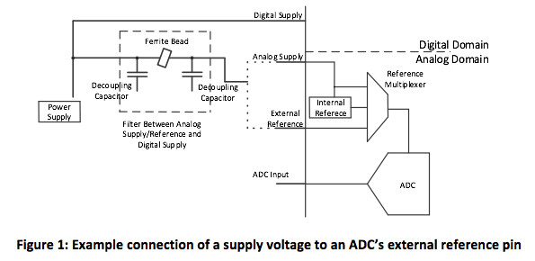
The supply as the reference is the lowest-current option but is usually noisier, as it supplies the digital circuitry (which has switching noise). One common technique to mitigate or protect the analog supply from digital switching noise is to use a filter between the analog and digital supplies if there are separate pins. Similarly, to isolate the noise on the supply from the reference, you could connect the external supply to the ADC’s external reference pin using a ferrite bead (a passive electric component) and decoupling filters to reduce the noise, as shown in Figure 1. A ferrite bead is common practice to isolate noise, especially between analog and noisy switching digital MCU power pins.
Reference [3] provides good details behind the use of a ferrite bead, and although it is written around a phase-locked loop (PLL), it is applicable to an ADC as well. Also, the supply used for the ADC reference generally cannot be a direct connection from a battery because the voltage will decay over the lifetime of the battery. You must know the ADC reference voltage to calculate the ADC’s converted voltage.
The internal reference typically provides lower noise than the supply at the cost of increased current consumption. Even when the supply has been filtered and applied to the external reference path as described above, the internal reference is typically a lower-noise option.
The conversion result from an ADC has meaning because the measurement is taken from the perspective of a reference. If the accuracy of the reference is poor, then the accuracy of the conversion result will be poor. Providing not only an accurate reference but a reference that is accurate over a wide temperature range is difficult to do in an embedded process, and is a good reason to consider an external reference.
External references are available with better accuracy and lower temperature coefficient/drift, which are generally the two dominate decision factors in choosing a reference. External reference voltages are available with a temperature coefficient in the single-digit parts per million per degree Celsius, while integrated MCU references range from 25 ppm/°C to 50 ppm/°C.
Table 2 provides an overview of the benefits and costs between internal (integrated) and external references. Reference [4] has more details on how to select a voltage reference and example error and accuracy calculations.
|
ADC reference
|
Advantage
|
Disadvantage
|
Suggested use
|
|
MCU supply
|
Lowest system current
No additional cost
|
Worst performance due to noise/
voltage dropped over the internal resistance (IR drop) from the ADC to the MCU power supply pin |
When the VDDA supply is not a battery and the lowest system power is a requirement
|
|
Internal REF
|
No additional cost
Medium performance
|
May need calibration technique vs. an external reference
|
When the VDDA supply does not meet performance
|
|
External REF
|
Best performance
|
Additional cost
Additional component
Usually higher current
|
When the best performance is a requirement
|
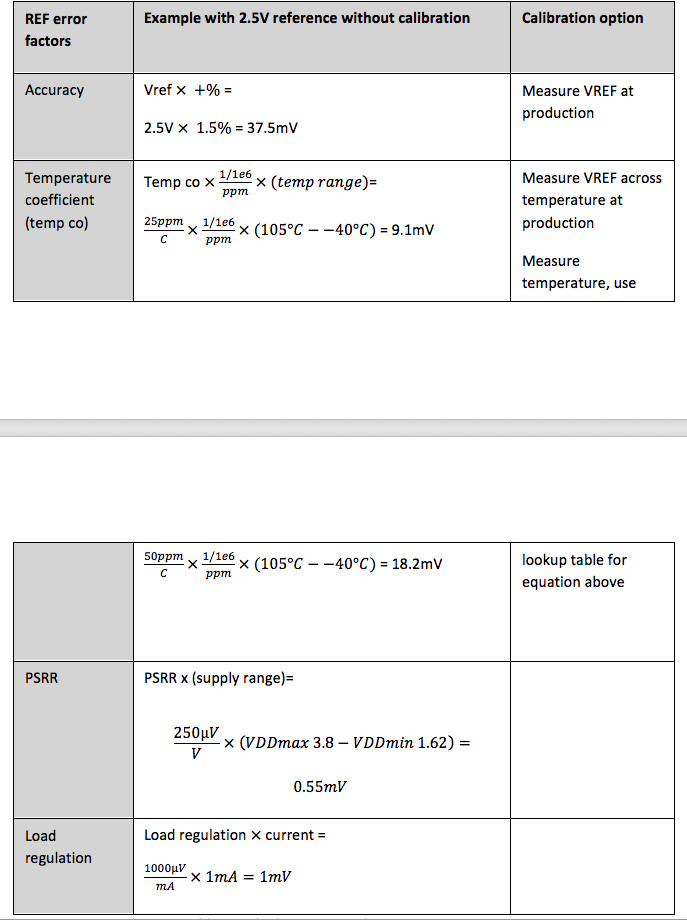
Typically, you’ll use the cheapest or lowest-power reference option that meets performance needs. To look at the required performance, consider these four main reference error factors:
- Accuracy – voltage change.
- Temperature coefficient – how much the voltage drifts over temperature. For temperature range, use your product’s temperature specification.
- Power-supply rejection ratio (PSRR) – how much the reference voltage changes across the device supply range that your application uses. If your application applies a regulated voltage to the MCU, this value is small (the ripple in the supply).
- Load regulation – if the reference is only going to the ADC, you can ignore load regulation. If not, use the total load from the voltage source used for the ADC reference.
You can use the calculation examples in Table 3 to help you calculate the required values.
There are two alternatives to using an external reference to improve DC reference accuracy across temperature:
- Calibration. Calibration is a multistep process that requires taking measurements in the production environment. In production, create a lookup table (or a single point if the temperature range is small) to determine the actual reference voltage (some device manufacturers actually measure this during device production and store it on-chip) and use the reference voltage in software to either correct the raw ADC code or adjust the ADC result for the inaccurate reference voltage. Equation 2 is the correction equation:
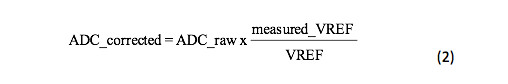
where VREF is the ideal ADC reference voltage and measured_VREF is the measured ADC reference voltage.
If you are correcting across temperature, you will need to take a temperature measurement at the time of the ADC measurement to know which measured voltage reference value to use in the lookup table. Table 3 shows some different reference parameters and the calibration options available to improve the parameters specifically for accuracy and temperature drift.
- Ratiometric measurement. In applications where the voltage used to excite the sensor is the same voltage used as the reference for the ADC, that measurement is called a ratiometric. By using the same voltage to excite the sensor and provide the ADC reference voltage, any error in the voltage will cancel out. For ratiometric measurements, you can use either an external reference or make an internal reference available outside the device. You can also take ratiometric measurements when a current source is used to excite the sensor with a resistor placed between the positive and negative ADC reference pins and the excitation current through that resistor. Reference [5] discusses an example of ratiometric measurement with a resistance temperature detector (RTD).
Conclusion
The clock and reference are two key components that impact ADC performance. When evaluating data-sheet performance and making comparisons to an actual design, it is important to appreciate the differences in the references and clock sources you select.
These first two installments focused upon why there is a difference between the data sheet and the actual design, highlighting the importance of test conditions and configurations. The next two installments will look at how to build a solution (a printed circuit board) that will align with the new expectations that come from a better understanding of the data sheet.
This is part two of a series, to read part three, click here.
References
- Neu, Thomas. “Clock jitter analyzed in the time domain, part 1,” Texas Instruments Analog Applications Journal, 3Q2010.
- Jitter and SNR Calculator for ADCs. Texas Instruments.
- Mustafa, Kal. “Filtering Techniques: Isolating Analog and Digital Power Supplies in TI’s PLL-Based CDC Devices,” Texas Instruments application report SCAA048, October 2011.
- Megaw, David. “Voltage Reference Selection Basics,” Texas Instruments (National Semiconductor) Power Designer article SNVA602, 2011.
- Hall, Christopher. “It’s in the math: how to convert an ADC code to a voltage (part 2),” Texas Instruments E2E™ Community blog post, April 29, 2016.