Using ESD Circuitry for all Your Woes? Buyer Beware!
June 24, 2019
Blog

The ESD (Electrostatic Discharge) internal transistors in your integrated circuits (IC), such as your amplifier, ADC, or DAC, can definitely save your bacon.
Yes, it is true. The ESD (Electrostatic Discharge) internal transistors in your integrated circuits (IC), such as your amplifier, ADC, or DAC, can definitely save your bacon. These handy IC transistors turn on, nearly instantaneously, during pre-assembly handling and assembly operations as protective devices. But be careful as you assume that these transistors will provide you with a comprehensive and ultimate protection. These transistors are designed to handle the transfer of electrostatic charge between bodies or surfaces at different electrostatic potential in high voltage (kV’s) environments and for a short duration event (1-100ns). Make no mistake. I am talking about an “out of circuit” event.
So, what happens if your device is soldered onto your PCB and the pin inputs or outputs linger slightly beyond the specified current or voltage limits? The key word in this question is “linger.” Your chip’s ESD transistors will very likely fail by shorting or opening up. This type of condition is called an Electrical Over Stress (EOS). A circuit in an EOS condition is subjected to currents or voltages beyond the IC’s maximum ratings. An EOS voltage is greater than the IC device pin’s specified voltage and is no longer a nearly instantaneous event. This type of event is a low-power, in-circuit occurrence and it interacts with the IC device’s internal circuits (Figure 1).
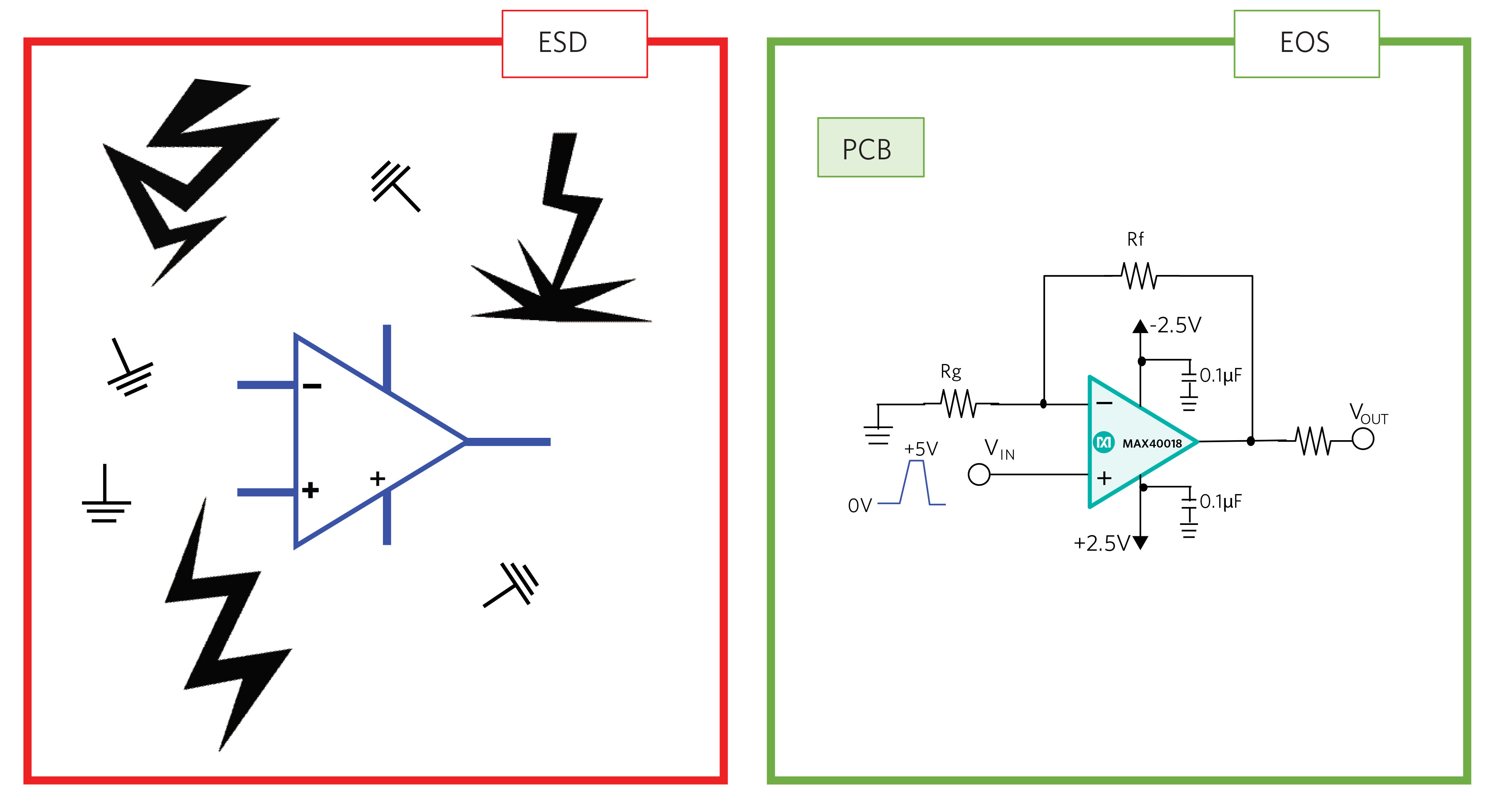
The set-up for an EOS event is easy enough to achieve. For instance, if you have unexpected electromagnetic interference (EMI) signal that impacts the high input impedance of an amplifier, you will see a surprising change in your signals (Figure 2).

In Figure 2, the low-power, CMOS MAX40016 amplifier is in a unity-gain or buffer configuration. The magnitude of the input signal to the amplifier, VIN, is within the specified input range. There is a second unexpected electromagnetic interference signal on the input (VEMI) that is transmitted and added into the input of the amplifier. An example where VEMI may occur is if you have a switching digital line in close vicinity on the PCB to the amplifier’s high-impedance input traces. The impact of this second, unwanted signal is devastating (Figure 3).
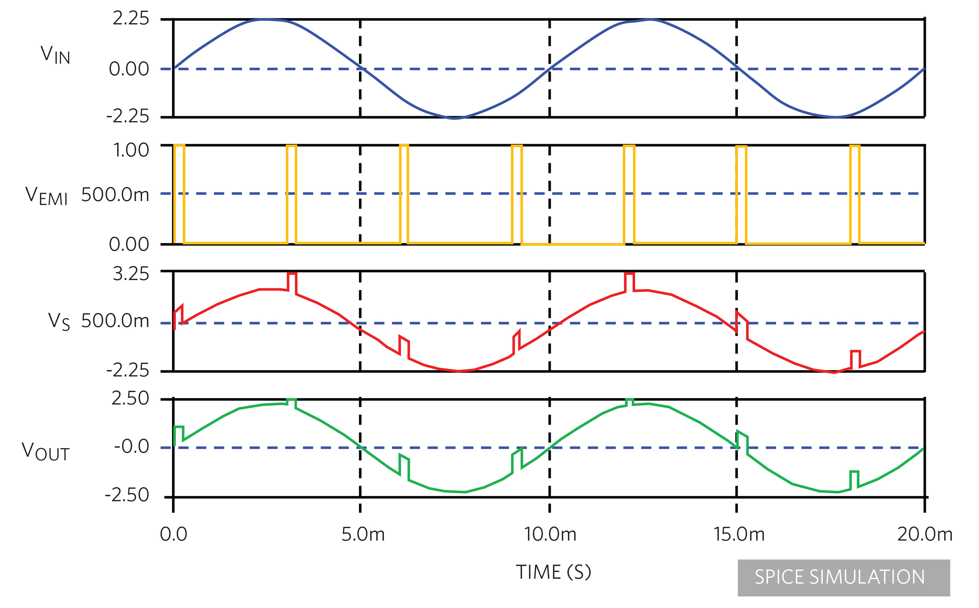
In Figure 3, VEMI contaminates the intended, low frequency signal (VIN). The voltage of VEMI plus VIN immediately exercises MAX40006’s CMOS input transistor. If the input signal is sufficiently large, the ESD circuit may be triggered by the input signal. For instance, with the first VEMI high signal (approximately 0.0 to 0.4 ms) the combined voltage remains within the MAX40006’s ±2.5 V power supply rails: no harm done. With the following VEMI spike to 1.0 V, the combination of VIN plus VEMI drives the MAX40006 input and ESD devices over the device’s maximum specifications for approximately 0.4 ms. This high voltage across the MAX40006 input transistors become very destructive short circuits to the positive power supply. Since Figure 3 shows simulated data we are not seeing the results of the possible physical damage that the MAX40006 experiences in real-life.
Integrated circuits, such as amplifiers, usually don’t include protection against EOS events. If you are lucky, the integrated electrostatic discharge (ESD) protection circuits activate during an EOS event and provide sufficient protection. The not so good news is that the ESD circuitry is not specifically designed to handle EOS conditions and may be damaged, beyond repair, during such an event. So, the preventative maneuver for this circuit is to make sure that EMI signal paths are mitigated.