How to Minimize EMI and Switching Loss When Using SiC MOSFETs
January 26, 2021
Story
The fast switching speed, high voltage rating, and low RDS(on) of silicon carbide (SiC) MOSFETs make them highly appealing for power designers who are constantly looking into ways to increase efficiency and power density, while maintaining system simplicity.
Yet, because their fast switching speeds produces high drain-source voltage (VDS) spikes with long ringing durations, they introduce EMI, particularly at high current levels.
Understanding VDS spike and ringing
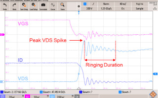
Parasitic inductance is the primary cause of VDS spike and ringing for SiC MOSFETs. Looking at the turn-off waveform (figure 1), the gate-source voltage (VGS) is from 18V to 0V. The drain current (ID), which is turned off, is at 50A, and the VDS is at 800V. The fast switching speed of the SiC MOSFETs causes a high VDS spike with a long ringing duration. This spike reduces the device’s design headroom to handle lightning conditions or sudden changes in load, and the long ringing duration introduces EMI. At high current levels, this event is more noticeable.

Figure1. VDS spike and ringing at turn-off with SiC MOSFETs (1200V 40mOhm)
Common EMI suppression techniques
The conventional way to suppress EMI is to lower the current flow rate through the device (dI/dt), which is achieved by using a high gate resistance (RG). But a high RG increases the switching loss significantly, and there is a compromise between efficiency and EMI.
Another way to suppress EMI is to lower the power loop stray inductance. However, to achieve this, the layout of the PCB needs smaller, less inductive packages. However, minimizing the power loop is limited, and the minimum spacing and clearance safety regulations need to be adhered to. Use of smaller packages also impacts the thermal performance.
The filter design can be used to help meet the EMI requirement and ease the system trade-offs. Control techniques, such as frequency dithering can also reduce the EMI noise from the power supply.
Using an RC snubber
Employing a simple RC snubber is a more effective and efficient approach. It controls VDS spike and reduces ringing duration with higher efficiency and a negligible turn-off delay. With faster dv/dt and extra capacitors, snubber circuits have a higher displacement current, which lowers the ID and VDS overlap at the turn-off transition.
The double pulse test (DPT) demonstrates the effectiveness of an RC snubber. It is a half-bridge configuration with an inductive load. Both the high- and low-side of the bridge use the same device, with VGS, VDS and ID measured on the low-side (figure 2). The current transformer (CT) measures both the device and the snubber current. The total measured switching loss, therefore, includes both the device and snubber losses.

Figure 2. Half-bridge configuration (same device for top & bottom)
The RC snubber is simply a 200pF capacitor and 10Ω resistor connected in series across the drain and source of the SiC MOSFET.

Figure 3: The RC snubber (left) controls turn-off EMI more effectively than high RG (right)
In figure 3, the turn-off for the same device in figure 1 is compared. The left waveform uses an RC snubber with low RG(off), whereas the right waveform has a high RG(off) and no snubber. Both approaches limit the turn-off peak spike drain-source voltage VDS. However, the snubber circuit is more effective by reducing the ringing duration to just 33ns, and the delay time is also shorter.

Figure 4. The comparison shows the using an RC snubber has very small impact at turn-on
Figure 4 compares the waveforms at an RG(on) of 5Ω with an RC snubber (left) and without. The turn-on waveform with the RC snubber has a slightly higher peak reverse recovery current (Irr), but there are no other noticeable differences.
The RC snubber controls the VDS spike and ringing duration more effectively than high RG(off), but does it impact efficiency?

Figure 5. Comparison of switching loss (Eoff, Eon) between snubber and high RG(off)
At 48A, the high RG(off) turn-off switching loss is more than double that of the snubber with low RG(off) and is almost comparable to that of the one without using a snubber. Therefore, it can be concluded that the snubber is more efficient, allowing faster switching and controlling VDS spike and ringing more effectively. Looking at the turn-on switching loss, the snubber increases the Eon only slightly.

Figure 6. Comparison of the total switching loss (Etotal) of snubber versus high RG(off)
To better understand the overall efficiency, Eoff and Eon are added together - Etotal (figure 6). When switching at full speed, the snubber is more efficient above 18A. For a 40mΩ device switching at 40A/40kHz, the difference in losses between high and low RG(off) with an RC snubber is 11W. To conclude, the snubber is a simpler, more effective and efficient method of minimizing EMI and switching loss than using high RG(off).
As 4th generation SiC devices enter the market, this simple solution will continue to enable engineers to design for optimal efficiency. For more information, watch UnitedSIC’s webinar - Minimizing EMI and Switching Loss for Fast SIC FETs.