Visualizing a 3D Circuit World Through KiCad
October 04, 2021
Blog

EDA packages like KiCad, and the design of electrical circuits in general, are normally thought of as a 2D affair.
Conceptually, this makes sense, as traces take a largely planar route from one connection to the next on a printed circuit board. However, we live in a 3-dimensional world, and being able to visualize circuitry this way, along with the corresponding components, is helpful in the design process. KiCad includes an impressive array of 3D viewing and export capabilities, which I’ll introduce in this article.
Basic 3D Viewing in KiCad
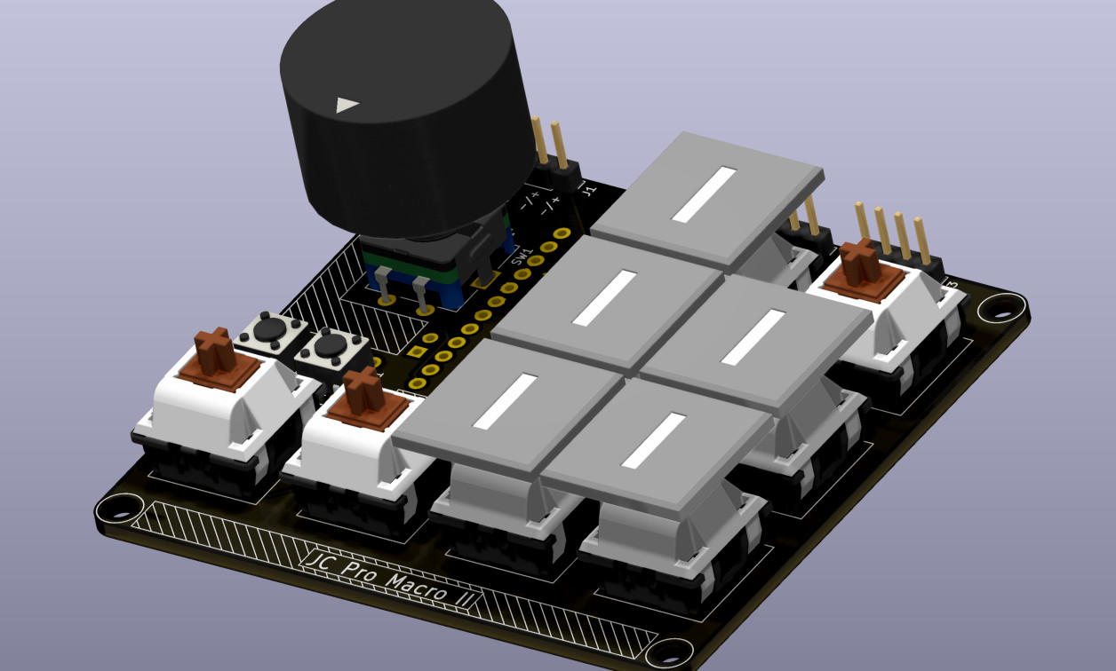
To view your PCB in 3D, open up Pcbnew, then select View > 3D Viewer. You’ll see your PCB in 3D, along with the components that are properly set up. In this interface, the middle mouse button pans, and the left button rotates the model. Right-clicking brings up a navigation window.
A variety of options and controls are available through this viewer. A few things you should explore include:
- Enable/Disable Orthographic Projection – (icon toolbar, gray 3D cube) Changes the view style. I generally prefer orthographic projection to be off.
- Render – (icon toolbar, blue 3D cube) Uses raytracing to produce a better image of the model. Quite slow for normal use, but great for screenshots.
- Preferences > Display Options – (menu bar in macOS) Lots of interesting options here. De-selecting Show board body can be especially useful to visualize vias and other intra-board elements.

Image Credit: Jeremy Cook (Screencap)
Edit and Create Component 3D Representations
When you lay out a circuit board, many of the default components will have 3D representations included. Some, however, do not. If you’d like to add a 3D model to an existing or new component, or modify what’s already there, this can be readily accomplished.
To edit a part on your board, select the component in the 2D layout mode of Pcbnew, then hit e to edit. Select 3D Settings, where you can modify the scale, rotation, and offset of the model. As seen below, I was able to use this as a rather rough-and-ready way to represent a dev board that is situated below the main PCB by adjusting the Z-offset.
Image Credit: Jeremy Cook (Screencap)
If you want to add in a different 3D model, you can delete any existing representation by selecting it in the edit screen, then hitting the trash can icon. Add a new .stl model by hitting the folder icon, then selecting it from its storage location. This location can technically be anywhere, but it’s good practice to store models for a project in a 3d_models directory within its folder.

Caption: That’s not standard!
Image Credit: Jeremy Cook (Screencap)
It’s also possible to modify a component’s 3D model through the Footprint Editor, via the Footprint properties (IC w/ gear) icon. This would be extremely useful when you’d like to use a model over and over. More information on how KiCad’s file structure works, and the different elements involved, is found here.
Export for External CAD Work
Just as printed circuit boards exist in three dimensions, they also rarely exist on their own, fixtured inside or on top of mechanical elements. The good news here is that your KiCad 3D model can be exported for use in a dedicated 3D CAD package. Select File > Export > STEP, which will produce a .stp file that can be used with a variety of programs.
In Fusion360, for example, you can then open the file via File > Open then selecting Open from my computer Find the proper .stp file, load it, and you’ll have a beautiful 3D model to build off of and modify. You’ll likely want to enable Capture Design History as shown in the image below for easier manipulations and back-tracking.

Per this example, if you do have a Fusion 360 subscription, the Autodesk EAGLE EDA package is also included and integrated with it. This should make this process easier of integrating electrical and mechanical components, though I haven’t worked with that program myself.
If I was starting from scratch, I might consider this workflow, but at this point I really enjoy using KiCad. I plan to stick with it for the foreseeable future and look forward to its continued development!
Jeremy Cook is a freelance tech journalist and engineering consultant with over 10 years of factory automation experience. An avid maker and experimenter, you can follow him on Twitter, or see his electromechanical exploits on the Jeremy Cook YouTube Channel!


