Take the Plunge into PCB Design
March 02, 2020
Blog

While I?ve been experimenting with circuits for years, decades even, my projects tend to be filled with a rat?s nest of wires. These snake about with the constant possibility of disconnection or other
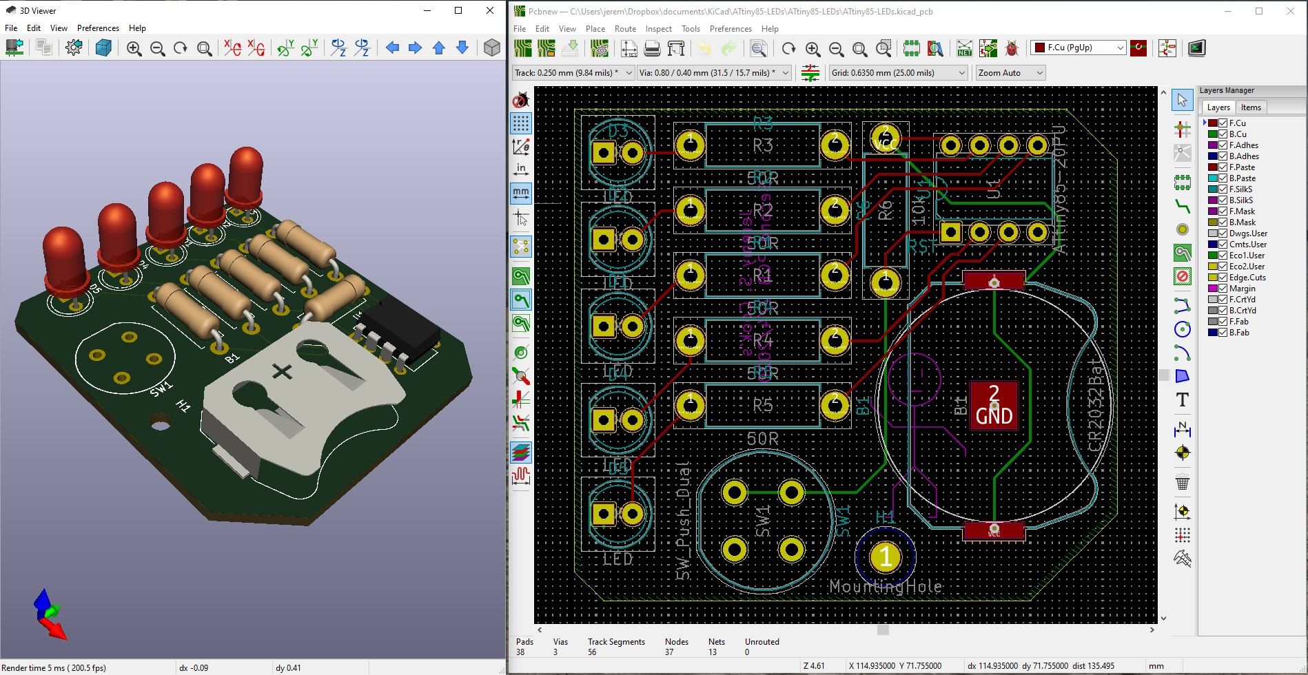
(Revised design on KiCAD - Image Credit: Jeremy S. Cook)
While I’ve been experimenting with circuits for years, decades even, my projects tend to be filled with a rat’s nest of wires. These snake about with the constant possibility of disconnection or other problems. They are a pain both to assemble and troubleshoot. Breadboards and perfboards are one possible solution, but I don’t particularly enjoy working with them, and they also tend to be quite messy in my case.
A final possibility is the printed circuit board, with precise connections from point-to-point made by a machine. This seems like a great solution, but to someone who has never made one, it also seems like a black art—something pursued by people much more competent than myself.
As someone that has recently designed two PCBs in the open-source KiCAD EDA platform, I know that this is not the case whatsoever. There is certainly a video tutorial out there somewhere to walk you through the process, this is what I recently used. I found these text instructions to be quite good, and going through it probably helped me remember things better.
What About Taking a Class?

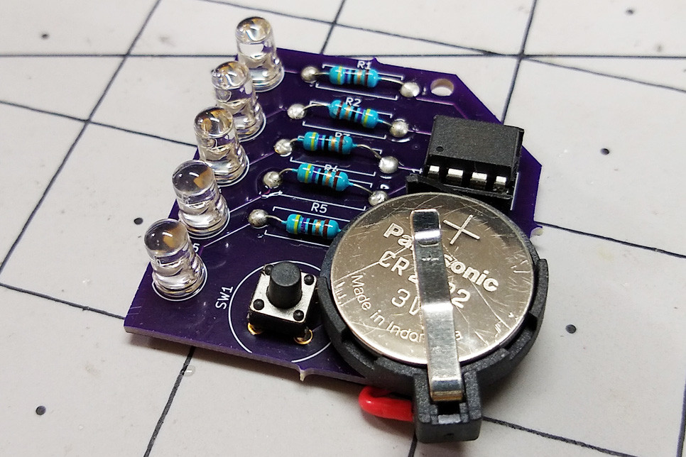
(Soldering my first design. Note mistake on CR2032 battery holder corrected by extra wire. - Image Credit: Jeremy S. Cook)
That being said, I’m not a total beginner with PCB design. Last May I took an intro to KiCAD class from Anool JM. While the class was excellent, I hesitated to implement what I’d learned immediately, perhaps in part because I was sure I’d forgotten something. Many months later, however, I imagine it did help me get through the starting guide. If you’re going to do such a class, make sure you have an easy project—one that you’ll actually order, a sort of “hello world” PCB—to work on immediately afterwards, otherwise your knowledge may be lost, or at the very least repressed.
Between the tutorial, and somewhat forgotten/repressed knowledge from the class, I was able to design and order an actual functional PCB from OSHPark. They specializes in this sort of experimentation, and you don’t actually have to mess about with Gerber or Drill files, but can upload KiCAD PCB files (*.kicad_pcb) directly to get them. Your design is priced instantly, and typically manufactured within a few days after the order is received.
While I was able to make a working PCB (with a correctable mistake on the battery holder footprint), I likely have neglected one or two things that Anool put out there as being good ideas during the class. If I was to do this over again, I think best way to take advantage of a class like this would be to stumble through an example or two and spend some time experimenting, then attend the class to help hone my technique. Hindsight, as they say, is 20/20.
Just Get Started!
Regardless of my sub-optimal learning order, I’m glad I finally took that intimidating first step of designing/ordering a board. My first PCB is not perfect by any means, but you can see three working copies of the design below. Each is a blinker powered by an ATtiny85, programmed to perform different actions.
Assembling my first "Hello World" PCB blinkie design!
Full video: https://t.co/BezmgAmzyu
Code: https://t.co/8Q3GGYkNw9
Designed in @kicad_pcb #ATtiny @oshpark @MicrochipMakes pic.twitter.com/CkzEL6kUHa
— Jeremy S Cook (@JeremySCook) February 25, 2020
Of course, I couldn’t stop there. My second design is a light following “robot,” which senses light via LDRs, causing the opposite motor to go forward and effectively chase light shined at it. I made this sort of light-follower in this video, but having a PCB should make things much easier. The boards were ordered, but have not arrived as of this writing. The first took about a week, but I believe this is on the short side time-wise for OSHPark.

(OSHPark ordering dialog for light-follower PCB. - Image Credit: Jeremy S. Cook)
Given how easy it is to make copies of such a board, I may set these up to sell on Tindie or elsewhere once I’ve verified that the follow-bot design works. There’s little downside for doing this, and this type of custom PCB setup could be a great step into manufacturing items for a profit.
Once you take this first step though, be prepared for a whole new world to open up for you. Already I’ve been considering using surface-mount (SMT) components in upcoming projects, and other ideas that I’d tossed aside for being too intricate from an electronics standpoint have been revived in my mind. It almost feels like I’ve taken the red pill to step out of the Matrix, revealing a world that I could sort of sense, but only interact with in a limited way.
__________________________________________________________________________________________________________
Jeremy S. Cook is a freelance tech journalist and engineering consultant with over 10 years of factory automation experience. An avid maker and experimenter, you can follow him on Twitter [https://twitter.com/JeremySCook], or see his electromechanical exploits on the Jeremy Cook YouTube Channel. [https://www.youtube.com/c/jeremyscook