Fundamentals of HBM, MM, and CDM Tests
June 10, 2019
Story

The primary ESD tests are the human-body model (HBM), the machine model (MM), and the charged-device model (CDM).
There are many established models that test the reliability of semiconductor devices against an ESD event to insure effectiveness and reliability. The primary ESD tests are the human-body model (HBM), the machine model (MM), and the charged-device model (CDM) (Figure1).
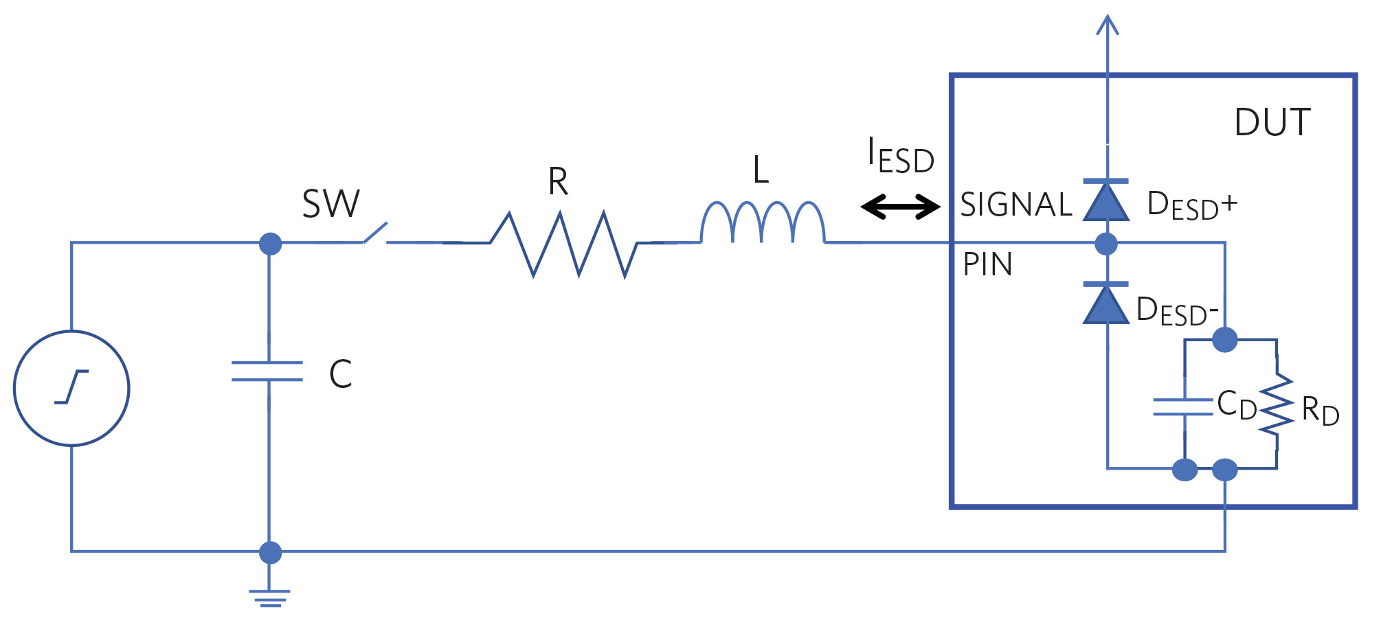
The JEDEC standards ensure ESD test effectiveness and reliability. The test configuration (Figure 1) for these three tests has five elements: VESD, C, SW, R, and L. The input VESD voltage charges the capacitor C before the closure of the switch (SW). With the closing of SW, the ESD fixture’s output impedance (R and L) sends the VESD signal, which converts to a current (IESD) into the device-under-test (DUT). The now ESD current flows through the DUT’s ESD diodes; DESD+ and DESD-. If either or both ESD diodes fail or are missing, the current (IESD) from this ESD event will find another path, which many times catastrophically goes further into the DUT circuitry.
Equation 1 represents the mathematical transfer function for the Figure 1 test circuit.

This configuration causes a momentary ESD event to occur at the Signal pin juncture to emulate one of the three ESD test signal events. The DUT Signal pin is either an input or output device pin. For these three ESD tests, the values of VESD, C, R, and L components vary to accomplish realistic ESD events (Table 1).
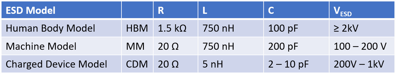
In Table 1, these three models boil down to a series RLC circuit plus a pulse generator, but the circuit values and pulse characteristics differ between the models. However, all three tests produce a short, well-defined ESD pulse that results in current (IESD) levels comparable to those experienced during an actual ESD event.
The human-body model (HBM) characterizes an electronic device’s susceptibility to electrostatic discharge (ESD) damage. The human body model is a model that simulates a human being’s ESD path from the finger through a device-under-test (DUT) and then to ground. The ESD supply voltage (VESD) charges the capacitor in the test circuit. The standard HBM test includes a supply voltage of ±2 kV, a high-value resistance at 1 to 10 M?, and a capacitance of 100 pF.
The intention of the Machine Model (MM) is to create an HBM test with more severity. The charge capacitor (C) is intentionally larger (200 pF), and the charge source resistance is a very low value; 0 to 10Ω. This low-value resistor allows the ESD source to supply even higher currents than the HBM model. Although the intention of this model is to characterize machine ESD events associated with the end-user electronic assembly, it is not intended to embody the handlers used in semiconductor final testing and handling.
The Charge Device Model (CDM) can be a replacement test for a one-time popularly applied MM. This CDM test simulates the charge accumulated by an IC package or piece of manufacturing equipment as a device is processed through the final production operations. In the manufacturing process, opportunities to create static electricity exist within the device handling equipment. This is where IC devices slide down anti-static tubes or test handlers that build up a charge.
The current (IESD) injected into the DUT generates heat. The magnitude of the generated heat depends on the peak ESD pulse voltage, the capacitance, and DUT resistance. In HBM testing, IC failure modes typically manifest themselves as gate-oxide, contact spike, and junction damage.
ESD Test Comparison
The similar rise times of these three tests are about 10 ns, but the total duration of the HBM and MM tests exceed the CDM model by approximately 200 ns (Figure 2).
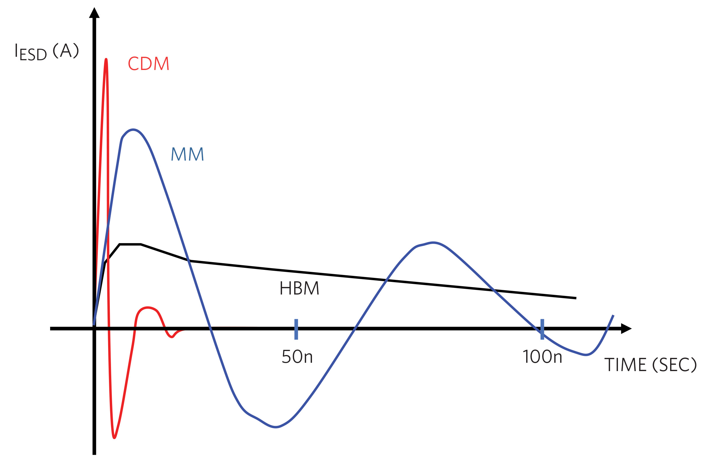
Figure 2 shows the current (IESD) waveform characteristics for HBM, MM, and CDM ESD tests. Usually, the stress level of the HBM ESD test is approximately 10 times higher than the MM ESD test condition. Also, the protection voltage level for HBM tests typically is 2 kV, while for MM tests, it is 200 V and for CDM tests, it is 500 V. There is no correlation between CDM, HBM, or MM. Therefore, HBM and CDM tests are commonly used for ESD protection circuit tests. The longer duration of IESD causes an increase in the overheating of the on-chip ESD structures. HBM and MM test failures usually show up in the gate oxide or as junction damage.
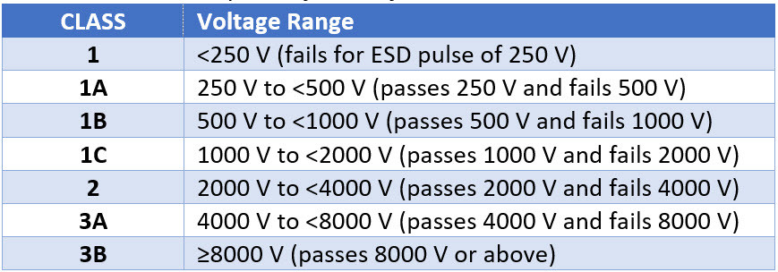
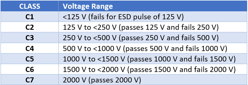
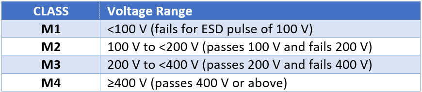
Tables 2, 3, and 4 show the HBM, CDM, and MM ESD immunity classifications.
References