How to Select a Boost Regulator/Controller IC and Select Peripheral Components – Part 3
April 22, 2021
Blog
In part 1 of this article series, we explored why switch current is important, what output current is required to satisfy expected loads, and the differences between selecting a buck and boost dc-to-dc converter.
In part 2, we looked at VSW, the transistor maximum allowable voltage and duty cycle limitation, how to understand peripheral stresses using LTspice, and the connection between VSW and duty cycle. In part 3, we will go into detail about peak current through and voltage across the inductor, current and voltage through the diode, and diode power dissipation.
To choose an inductor for your boost application, you need to know if the inductor can handle the currents and voltages it will face—namely the peak inductor current, and the TON and TOFF voltages. This can also be estimated in LTspice using differential probes. To probe differentially across the inductor, hover over the IN node, and the crosshair cursor will change to a red probe. Click and drag the mouse to the SW node. The cursor color changes to black. Release when over the second node.
In Figure 15, the voltage between nodes IN and SW are probed differentially across the inductor. During TON, the MOSFET conducts, so the right side of the inductor is near ground, while the left side is at VIN, making the voltage across the inductor 12 V during TON. During TOFF the MOSFET is off, placing the right side of the inductor at 48 V, while the left side is at VIN, as during TON. Because the differential probe subtracts VSW from VIN, the result is –36 V, but the sign is irrelevant (for now). What is important is that the inductor changes between 12 V and 36 V.
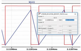
During TON, the voltage across the inductor draws a positive di/dt, the slope of the blue I(L1) graph. The maximum point of this trace is IPEAK, calculated as 0.847 A. Using LTspice, we can see that the peak current is about 866 mA.
The peak current is important to know in order to properly choose an inductor with sufficient rated current (IR) and saturation current (ISAT). IR is more about how much heat is generated at the stated current, and ISAT applies to events invoking short-circuit protection. If a regulator with internal MOSFETs is used, (ISAT > regulator current limit), and if a controller is used with external MOSFETs, then (ISAT > the peak inductor value) when the current limit is triggered.
It is important to note that the boost topology as described here has no current limit for the inductor or diode. If the switch is not used, or the IC is off, there is a direct path between input to output. There are ICs that provide additional protection features, such as output disconnection in shutdown, inrush current limiting, and other features to address this direct input to output connection—for example, the LTC3122 and LTC3539.
To improve efficiency, inductors featuring low DCR (dc resistance) and low core losses should be used. DCR is noted in the inductor data sheet at a particular temperature—it rises with temperature and has a tolerance. The dc losses can be easily computed from PINDUCTOR_LOSS = IIN_AV² × DCR, while the ac losses and core losses can be found in manufacturers’ simulation or other documentation. LTspice can integrate power to calculate associated power loss. Providing LTspice with an inductor’s documented DCR and other known parasitic parameters improves LTspice simulation accuracy.

Figure 15. Voltage and current through the inductor at steady state.

Figure 16. Measuring the inductor peak current.
Current and Voltage Through the Diode
Figure 17 shows the simulated differential voltage across the diode VSW,OUT, the diode forward current I(D1), and the inductor current I(L1). When the switch is on (during TON), the anode is close to ground and the cathode is at the output voltage, so the diode is reverse biased and exposed to its maximum voltage, namely VOUT. Selecting a diode that has VRRM (maximum peak repetitive reverse voltage) higher than VOUT is the first criteria.
The inductor’s peak current flows through the diode once the MOSFET is turned off, at the commencement of the TOFF period, so the diode peak current is the same as the inductor peak current. The diode data sheet includes a parameter called IFRM, the repetitive peak forward current, specified at a time duration and duty cycle. This parameter is usually higher than the average current the diode can provide.
After simulation is completed, LTspice can integrate any waveform in the waveform viewer to produce rms and average values and, by the same measure, the average current the diode will face. First, zoom in on the part of the waveform you want to integrate—zooming effectively sets the integration bounds. In this case, you want to zoom to cover a significant number of steady state cycles (not startup or shutdown). To set the integration bounds, drag over a steady state time period and hover over the graph name. For instance, the integration result shown in Figure 18 covers 0.75 ms, or over a thousand cycles. The cursor changes to a hand icon. Press the CTRL key and click to invoke the integration window of the waveform viewer.
The integration dialog box shown in Figure 18 displays the average current through the diode, which is 150 mA. This should be less than the IF(AV), maximum average forward current, specification in a diode data sheet, usually stated at a specific case temperature.
Diode Power Dissipation
The power dissipation of the diode can also be computed from the simulation. A diode data sheet specifies PTOT (total power), the total power dissipation at 25°C, and RTH, the junction-to-ambient thermal resistance. In LTspice, the power dissipation can be displayed on the waveform viewer by hovering over the diode; when you hover over a body of a discrete component or a voltage source, the mouse cursor changes to a current probe. Press the ALT key to change the cursor to a thermometer and click to show the simulated power dissipation over the diode. Zoom in on steady state operation to integrate the waveform using the same procedure as previously described for the integration of the diode current. Diode power handling comprises the voltage across the diode and the current that flows through it.

Figure 17. Diode voltage and current along with the current in the inductor.

Figure 18. Integration of diode current in steady state provides IF(AV) and I(RMS) values.

Figure 19. Integration of power dissipated by the diode to yield average power dissipation.

Figure 20. Reverse recovery spike cause at the diode discharge. A lower value means lower power loss. This capacitance changes with voltage. (a) Diode reverse recovery current spike. (b) Zooming in on the diode reverse recovery current spike.
The diode has some capacitance that is charged during its conduction period. The accumulated charge must be discharged when the diode no longer conducts. This damped charge movement results in loss of power, so selecting a low capacitance value is recommended. This capacitance value changes with the diode’s reverse voltage, and a diode data sheet should include a graph displaying this effect. This internal capacitance is typically shown in diode data sheets as Cd and in the LTspice database as Cjo.
Using a low capacitance diode relaxes the requirements of the maximum reverse recovery current, improving efficiency. Figure 20 shows what to look for regarding recovery current. The power dissipation inherent in the reverse recovery is left as an exercise to the reader.
Conclusion
When selecting a boost IC, start at the output. Work backward from the desired output voltage and load current to find input power, taking efficiency into account. From this, determine the average and peak input current values. In a boost, the average current flowing in the inductor is higher than the load current, making the IC selection process different from that of a buck. Choosing properly rated components for a boost converter requires knowledge of the regulator peak and average voltages and currents, which can be determined using LTspice.

Rani Feldman joined Analog Devices in 2017 as a senior field applications engineer. Previously, Rani worked for Linear Technology for three years. Rani has a bachelor’s degree in electronics engineering from Afeka College in Israel and holds a master’s degree in business and administration from Holon Institute of Technology in Israel.