How to Select a Boost Regulator/Controller IC and Select Peripheral Components – Part 1
April 16, 2021
Blog
The process of selecting an IC for a boost regulator is different than that for a buck regulator, where the main difference lies in how desired output current relates to regulator IC data sheet specifications.
In a buck topology, the average inductor current is essentially the same as the load current. This is not the case for a boost topology, which requires calculations based on switch currents. This article series will cover both the selection criteria for a boost regulator IC (with internal MOSFET) or a controller IC (with external MOSFET), and how to use LTspice to select appropriate peripheral components to complete the boost power stage. In part 1, we will explore why switch current is important, what output current is required to satisfy expected loads, and the differences between selecting a buck and boost dc-to-dc converter.
Why switch current is important
What are the input and output voltages? This is the first question one asks when selecting a buck (step-down) or boost (step-up) dc-to-dc converter. The second question: what is the output current required to satisfy expected loads? Even though the input and output questions are the same for bucks and boosts, the process of selecting a suitable IC to satisfy input and output requirements is very different between bucks and boosts.
The first hint that the selection process for boosts is different from that for bucks is apparent if you compare a selection table of buck ICs vs. a selection table of boost ICs. Figure 1 shows the selection table for some internal power switch bucks. It can be seen that output current gets billing as one of the main selection parameters.

Figure 1. Internal power switch buck selection table showing the output current as a selection parameter.
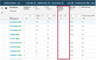
Compare Figure 1, a selection table of internal power switch bucks, to Figure 2, a selection table of internal power switch boosts. In the boost table, output current does not even show up as a selection parameter, making way for switch current instead.

Figure 2. Switch current shows up as a parameter in a selection table for a boost converter IC, instead of output current.
Another clue that boosts don’t follow the same rules is the data sheet title, which for a boost, has a subtle but important statement about current. For example, Figure 3 shows the front page of the data sheet for the LTC3621 monolithic buck, where 17 V max VIN and 1 A continuous load capability are prominently noted.

Figure 3. The LTC3621 buck regulator data sheet front page shows max typical operating voltage and current.
In contrast, the title of the data sheet for the LT8330 monolithic boost states the max voltage (60 V) and current (1 A) for the switch (the internal power MOSFET), instead of the typical maximum values for the load current and input voltage. You can also see that for a boost the input voltage range of 3V to 40V differs from the 60V max switch voltage.

Figure 4. The LT8330 boost regulator IC data sheet front page shows max power switch capabilities.
So, why the difference? In a buck regulator, the average inductor current is about equal to the output (load) current, whereas in a boost topology, this is not the case. Let’s look at why by examining the boost topology in comparison to a buck.

Figure 5. An asynchronous boost.
Figure 5 shows the simplified schematic for an asynchronous boost topology, and Figure 6 shows the simplified schematic of an asynchronous buck topology. The D block for both is the PWM signal that drives the power MOSFET, with the duty cycles of switching periods determined by the input and output voltage ratio. In this article, to keep it simple I am using lossless continuous conduction mode (CCM) equations as they provide close enough results.

Figure 6. Asynchronous buck regulator simplified schematic.
By using LTspice, we can clearly see the difference between the input and output currents of the two different topologies. Figure 7 shows a basic open-loop design for a buck, converting a 12V input to a 3.3V output that will provide 1A (3.3W) to the resistive load, R1. The PWM D block is implemented by V2, a floating supply, as we need VGATE > VSOURCE to establish conduction for the N-channel MOSFET, M1. V2 is used as a PULSE voltage source to implement a 0 V to 5 V pulse, which begins at time 0 of the simulation, transitions from 0V to 5V in 5ns and back down again in 5ns with a TON of 550 ns, while TP (full switching period) is equal to 2 µs.

Figure 7. A buck regulator open-loop topology converting 12 V to 3.3 V at 1 A—an approximately 3 W design.
After running the simulation of the circuit in Figure 7, it is possible to probe the currents of L1 and R1. The current in L1 has a triangle shape as it charges and discharges due to the switching of M1 according to the timing of TON, the time M1 is on, and TOFF, the time M1 is off.
The L1 current switches at a 500 kHz switching frequency. We can see that the inductor current is an ac + dc waveform. It transitions from a minimum value of 0.866 A (end of TOFF) to a maximum value of 1.144 A (end of TON). As ac signals look for the path of least impedance, the ac portion of the current flows through the ESR of output capacitor C2. This alternating current, along with the charging and discharging of C2, results in output voltage ripple, while the direct current flows via R2.
Comparing the triangular shapes of the inductor current formed above and below the load current, we can see they are equal, and simple algebraic calculation shows that:
The average inductor current is equal to the load current.

Figure 8. Buck topology—inductor current and load current simulation example.
When searching for a buck regulator IC, it is safe to assume the data sheet shows the maximum allowed output current, as IIN ≈ IOUT, but this is not the case for the boost topology.
Let’s look at Figure 9, which shows an open-loop boost design for a 3.3 V input to a 12 V output at 0.275 A, or about 3.3 W. What is the average inductor current in this case?
In Figure 10, the output current is the dc trace at 291 mA, I(R2)—close to what was computed. While the simulated load current is 291 mA, the simulation shows that the inductor current has an average value of 945 mA and a peak value of more than 1 A. This is more than 3.6 times the output current. During TON—the time in which M2 is conducting, and there is a voltage of V3 across L2—the inductor charges from its minimum value to its maximum value. During TON, D2 is off and the load current is provided by the output capacitors.
During TON, the inductor is in series with the MOSFET, so any current flowing through the input inductor flows through the switch. Because of this, the data sheet specifies the maximum current that can flow through the switch, ISW. One should know the expected maximum current through the switch (and the inductor) when selecting a boost IC for a new design.
For example, take a boost regulator for the following application:
-
VIN = 12 V
-
VOUT = 48 V
-
IOUT = 0.15 A
Choosing the correct boost regulator requires one to find the average input current, as this is the current that flows through the inductor and MOSFET during TON. To find this current, work backward from output to input according to output power and efficiency:
-
POUT = VOUT × IOUT = 48 V × 0.15 A = 7.2 W
-
Assume an efficiency of 0.85 (or use the data sheet if there is an efficiency curve with similar input and output parameters to the desired design).
-
PIN = POUT/efficiency = 7.2 W/0.85 = 8.47 W
-
IIN_AV = the average input current. This is the same average current that flows in the inductor and switch during the on-time, which is calculated by PIN/VIN = 8.47 W/12 V = 0.7 A.
-
Again, IIN is the average inductor current, the maximum peak current will be 1.15 to 1.20 higher than IIN, allowing for 30% to 40% of ripple current. So, IPEAK = IIN × 1.2 = 0.7 A × 1.2 = 0.847 A.

Figure 9. Boost topology: 3.3 V to 12 V, approximately 3.3 W.

Figure 10. LTspice simulation result for open-loop boost from 3.3 V to 12 V at 0.275 A.

Figure 11. Schematic during TON: M2 is on, V3 is in parallel to L2, and D2 is off.
In part 2, we’ll look at VSW, the transistor maximum allowable voltage and duty cycle limitation, how to understand peripheral stresses using LTspice, and the connection between VSW and duty cycle.

Rani Feldman joined Analog Devices in 2017 as a senior field applications engineer. Previously, Rani worked for Linear Technology for three years. Rani has a bachelor’s degree in electronics engineering from Afeka College in Israel and holds a master’s degree in business and administration from Holon Institute of Technology in Israel.