How to Program a Lock-in Amplifier
April 21, 2022
Blog
The lock-in amplifier can extract excessively low signals in the presence of relatively high noise. In recent years there has been increased interest in portable or embedded lock-in amplifiers for instrumentation and sensing purposes.
1. Introduction
The fundamental approach of lock-in amplifiers is to make the physical value to be measured periodic. By shifting the DC signal in this way to a known frequency, one can avoid high levels of low-frequency flicker noise. Due to the unique phase-sensitive detection of the lock-in amplifier, the output voltage signal will provide very precise information about the measured physical value even if a high level of noise is present.
Lock-in amplifiers have wide use in applications where low-level signals are corrupted by high noise. With a low-voltage and low-power measurement system that can be easily battery powered, the field of application can be broader yet.
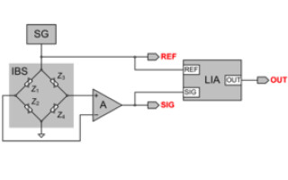
A typical application of the lock-in amplifier is presented in Figure 1, where the lock-in amplifier (LIA) is used to demodulate the signal obtained from an impedance bridge sensor (IBS). The reference source (REF) is usually a reference periodic signal that can be obtained from the signal generator (SG) or some other periodic signal source. This REF source also powers the sensor. The signal source (SIG) is an output from the sensor, and it has the same frequency as the REF source. It is typically obtained at the output of the sensor amplifier (A).

Figure 1: Typical Application of a Lock-in Amplifier
Based on the two synchronized signals (REF and SIG) the lock-in amplifier generates a slowly varying output signal (OUT) that corresponds to the measured value of some physical parameter, such as temperature, whereas all other interfering signals are significantly suppressed.
2. Principle of Operation
The lock-in amplifier presented herein is composed of a demodulator circuit that, with the help of an operational amplifier, two switches, and several passive components, changes the amplifier gain between +1 and -1 during one period of the reference signal (REF). This is presented in Figure 2. When the REF signal is larger than its time-averaged value the amplifier gain is +1, and when the REF signal is smaller the amplifier gain is -1. The demodulated signal is fed into the circuit that performs low-pass filtration and amplification. In this way, one obtains a voltage signal at the lock-in amplifier output that is proportional to the sensor signal amplitude. Moreover, with the help of two rheostats and additional components, one can adjust the filter bandwidth and gain.

Figure 2: Principle of Operation of the Lock-in Amplifier
To demodulate the sensor signal (SIG), one must multiply this signal with the reference signal (REF). This is typically performed with the help of an analog voltage multiplier circuit. If an analog voltage multiplier isn’t available, one can perform the multiplication by switching the sign of the amplifier gain synchronously with the reference signal.
For that purpose, one must provide two digital signals S1 and S2 at the output of the comparator C as presented in Figure 2. When the reference signal is larger than its time-averaged value, S1 = 1 and S2 = 0. In the opposite case, when REF is smaller than its time-averaged value, S1 = 0 and S2 = 1. These two digital signals further drive the switches SW1 and SW2. The capacitor CR1 = 100 nF and the resistor RR1 = 100 kΩ are chosen to simply suppress the DC value of the reference signal.
The amplifier gain switching is performed with the help of the operational amplifier OA1, two switches SW1 and SW2, and several passive components. When switch SW1 is closed (S1 = 1) and switch SW2 is open (S2 = 0), the amplifier gain is +1, i.e. the voltage signal at the output of the operational amplifier OA1 is equal to the AC part of the input sensor signal (SIG). In the opposite case, when switch SW1 is open (S1 = 0) and switch SW2 is closed (S2 = 1), the amplifier gain is -RS2/RS1 = -1, i.e. the voltage signal at the output of the operational amplifier OA1 is equal to the inverted AC part of the input sensor signal (SIG). The capacitor CS = 100 nF filters the sensor signal's DC part, whereas the capacitor CS2 = 10 pF provides amplifier stabilization.
The resistor RL = 100 kΩ has the same value as the resistor RS1 = 100 kΩ to load the capacitor CS with the same load during both half-cycles of the reference signal (REF) and thus provide undisturbed current flow. To provide maximum swing of the output voltage, a reference voltage of VR = VDD/2 = 1.65 V, i.e. one half of the power supply voltage (VDD = 3.3 V), is provided to the non-inverting input of the operational amplifier OA1. In this case, one has the maximum overall swing of 3.3 V for both cases when the sensor signal (SIG) is in phase with the reference signal or it is inverted with respect to the reference signal.
The output of the operational amplifier OA1 is a rectified replica of the sensor signal (SIG). This signal must be further filtered to obtain a slowly varying counterpart of the measured physical value (such as temperature). The filtration is performed with a low-pass filter realized with the help of the second operational amplifier OA2 and several passive components. The second-order low-pass filter has a well-known Sallen–Key topology, for which bandwidth and gain can be adjusted with the help of two rheostats RR1 = 100 kΩ and RR2 = 100 kΩ, respectively. All passive components are chosen such that the gain can be set in a range between 1 and 11, and the bandwidth between approximately 1 Hz and 10 Hz.
The filter gain is given by K = 1+RR2/RG, where
- RR2 = 0 – 100 kΩ
- and RG = 10 kΩ.
The gain is between 1 and 11, providing an order of magnitude of gain change.
The filter bandwidth is given by
B ≈ 1/(2π((RF1+RR1)RF2CF1CF2)1/2), where
- RF1 = 1 kΩ,
- RR1 = 0 – 100 kΩ,
- RF2 = 100 kΩ,
- CF1 = 10 μF, and
- CF2 = 100 nF.
The bandwidth is between 1.6 Hz and 16 Hz, providing an order of magnitude of bandwidth change.
The quality factor (Q-factor) is given by
Q = ((RF1+RR1)RF2CF1CF2)1/2/((RF1+RR1+RF2)CF1+(RF1+RR1)CF2(1-K)), which should be positive in order to provide a stable response.
This is fulfilled for (RF1+RR1+RF2)CF1+(RF1+RR1)CF2(1-K) > 0
or
K < 1+(RF1+RR1+RF2)CF1/((RF1+RR1)CF2), which in the worst case scenario for
RR1 = 100 kΩ gives K < 200, which is fulfilled even for the maximum filter gain of 16.
Finally, the capacitor CR2 = 100 pF is employed for amplifier stabilization.
2.1 Circuit Realization
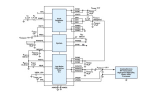
This lock-in amplifier was realized with the help of the GreenPAK™ SLG47004 Programmable Mixed-Signal Matrix as presented in Figure 3(a). Besides the passive components described above, two push buttons have been employed (BS and GS) to set the bandwidth and gain of the lock-in amplifier. The circuit is realized in such a way that when each of the buttons is pushed, the internal rheostat value is set to the initial value. Then, depending on how long the button is pushed, the rheostat value is changed and set to the desired value.
Resistors RBS1 = RGS1 = 10 kΩ and RBS2 = RGS2 = 100 kΩ, and capacitors CBS = CGS = 100 nF were chosen to suppress the potential voltage pulses due to the switch bounce. Moreover, the pins I0 (pin 21) and IO1 (pin 15) are configured as digital inputs with a Schmitt trigger. Pin IO0 (pin 12) is connected via resistor RB = 7.5 kΩ to ground to provide current sourcing from this pin, since the internal voltage reference VR = VDD/2 = 1.65 V is connected to this pin and it can only source the current. Capacitors CB1 = 10 μF and CB2 = 100 nF serve for the power supply filtration.
Finally, to generate the corresponding sensor signal (SIG) (in this case, for pressure measurement), the reference signal (REF) is brought via the capacitor CW = 1 μF for the potential DC signal blocking of the reference signal to the Wheatstone bridge. This is the integral part of the PA-9 pressure sensor (from KELLER AG für Druckmesstechnik, Switzerland) which is further composed of four pressure variable resistors RP1 = RP2 = RP3 = RP4 = 3.5 kΩ ± 20%, as presented in Figure 3(b).
The amplification of the corresponding pressure sensor signal is performed with the help of the SLG88103 Rail to Rail I/O 375 nA Dual OpAmp operational amplifiers and several passive components. To set the amplifier common-mode voltage to approximately one half of the power supply voltage, and thus to provide the maximum possible sensor dynamic range, the power supply voltage +VDD = +3.3 V is brought via two resistors RL1 = RL2 = 3.6 kΩ to the inverting and the noninverting inputs of the first operational amplifier (OA1). Therefore, the values of the resistors RL1 and RL2 are as close as possible to the measurement bridge resistance RP = 3.5 kΩ (RL1, RL2 ≈ RP).
The first amplifying stage gain is set with the help of the resistor RA = 18 kΩ to the value equal to G1 = -(RA/RP)(1+RL2/RL1+RL2/RA) = -11.3. The first stage gain was chosen to be approximately -10 to satisfy the bandwidth requirements of approximately 1 kHz since the SLG88103 operational amplifier has a low gain-bandwidth product (~ 10 kHz). To provide larger bandwidth amplification, one must use other operational amplifiers with larger gain-bandwidth products. Since the gain of the first amplifying stage is not sufficient for sensor signal amplification, the second amplification stage is realized with the second operational amplifier (OA2) and several passive components having a gain of G2 = -RA2/RA1 = -10. Capacitor CA = 1 μF serves for the potential DC signal blocking, since due to the sensor resistors mismatch, there will be a small DC signal at the output of the first amplifying stage. Resistors RL3 = RL4 = 10 kΩ set the second stage amplifier common-mode voltage at one-half of the power supply voltage, thus providing the maximum possible dynamic range.

(a)

(b)
Figure 3: Circuit Realization of the Lock-in Amplifier and (b) Pressure Sensor with the Amplifying Stages
The lock-in amplifier circuit was designed and tested with the help of GreenPAK Designer as presented in Figure 4. The action of the push buttons BS and GS are modeled with equivalent voltage sources, whereas the reference signal (REF) and the sensor signal (SIG) are modeled as sinusoidal signal generators. The corresponding pin settings are given in Table 1, and the corresponding macrocell settings are presented in Figure 5 to Figure 15.
This design was created using free GUI-based GreenPAK Designer software (a part of the Go Configure™ Software Hub). The complete design file is available here.

Figure 4: Lock-in Amplifier circuit in GreenPAK Designer

Table 1: Pin Settings

Figure 5: OPAMP Settings

Figure 6: Digital Rheostat Settings

Figure 7: CNT1/DLY1 and CNT3/DLY3 Settings

Figure 8: CNT2/DLY2 and CNT4/DLY4 Settings

Figure 9: 2-bit LUT2/DFF/LATCH2 Settings

Figure 10: 2-bit LUT3/PGEN Settings

Figure 11: OSC0 Settings

Figure 12: SWITCH Settings

Figure 13: 2-bit LUTs/DFFs/LATCH Settings

Figure 14: ACMP0L Settings

Figure 15: VREF0 Settings
2.2. Simulation Results
A series of simulations were performed to test the circuit functionality. Figure 16 shows the simulation results obtained at the outputs of both operational amplifiers. The first time diagram represents the reference signal (REF), the second time diagram represents the sensor signal (SIG), the third time diagram represents the rectified sensor signal, and the fourth time diagram represents the demodulated signal at the lock-in amplifier output, i.e. the amplified and filtered rectified signal.

Figure 16: Simulation Results from the Outputs of Both Operational Amplifiers
Figure 17 presents the simulated time diagrams for the corresponding signals targeting the bandwidth settings.

Figure 17: Time Diagrams of the Corresponding Signals Targeting the Bandwidth Settings
The first-time diagram seen above represents the signal obtained from the signal generator BS that simulates the action of the push button BS (as seen in Figure 3). The second time diagram represents the signal at the output of the 3-bit multi-functional LUT (CNT1/DLY1), which generates a delayed single shot that reloads the initial value to the digital rheostat RH0 stored in the MTP NVM. The third time diagram represents the counts at the digital rheostat RH0 CLK input that increase the rheostat resistance to the desired value. Finally, the fourth signal represents the digital rheostat RH0 resistance code.
Figure 18 presents the simulated time diagrams of the corresponding signals targeting the gain settings, with similar signals as in the previous case. The only difference is that the digital rheostat RH1 targets the lock-in amplifier gain settings.

Figure 18: Time Diagrams of the Corresponding Signals Targeting the Gain Settings
2.3. Experimental Results
The lock-in amplifier circuit as presented in Figure 3 was realized to test its complete circuitry. The signal generator output signal, i.e. the reference signal (REF), is presented in the first time diagram in Figure 19 and shows the captured oscilloscope screen. The sensor signal (SIG) is presented in the second time diagram, the rectified signal (RS) at the output of the first operational amplifier is presented in the third time diagram, and the fourth time diagram represents the demodulated signal at the lock-in amplifier output (at the output of the second operational amplifier), i.e. the amplified and filtered rectified signal (OUT).
To test the action of the gain change, the GS push button is kept turned on for a couple of seconds, thus increasing the gain of the lock-in amplifier. The corresponding lock-in amplifier output signal is amplified as presented in Figure 20, where the fourth time diagram has a higher level compared with the corresponding signal of the fourth time diagram presented in Figure 19.

Figure 19: Oscilloscope Time Diagrams of the Corresponding Lock-in Amplifier Signals

Figure 20: Oscilloscope Time Diagrams of the Corresponding Lock-in Amplifier Signals with Increased Gain
The most prominent feature of the lock-in amplification is the suppression of the high levels of low-frequency flicker noise, which cannot be seen from above. The above measurements aim to prove the concept of the lock-in amplifier as designed.
To test the flicker noise suppression of the lock-in amplifier, a long-term stability test of the circuitry was performed. The output lock-in amplifier voltage signal (OUT) was recorded for 24 hours. During the measurement, the pressure sensor was located inside an airtight vessel, which is hermetically isolated from the surrounding environment to keep constant pressure and thus eliminate potential measurement error due to atmospheric pressure variations. The output signal (OUT) was sampled with the help of a 12-bit digital acquisition card with a sampling frequency of 2 Hz (the bandwidth of the lock-in amplifier was set to the minimum value of approximately 1 Hz). The power spectral density (PSD) of the measured output noise signal, which is obtained by subtracting the measured output signal (OUT) and its time-averaged value, is presented in Figure 21.

Figure 21: Power Spectral Density (PSD) of the Measured Output Noise Signal
The power spectral density (PSD) ranges from 10 μHz up to 1 Hz, which is in the range of the flicker noise of the operational amplifiers. One can expect that in this range we have an increase in the noise power spectral density starting from 1 Hz and going toward lower frequencies. However, this cannot be observed in the measured output noise power spectral density. Moreover, the power spectral density decreases when approaching lower frequencies to approximately 1 mHz. There is only an increase in the power spectral density at very low frequencies (~10-4 Hz – ~10-5 Hz). The reason for this increase lies only in the limited measurement time (measurement was performed for 24 hours) as well as the possible change of pressure inside the airtight vessel due to the slight temperature changes inside the room during measurement.
Besides the suppression of flicker noise, the lock-in amplifier exhibits very high immunity to interfering signals that may significantly disturb measurements. To demonstrate this immunity, the interfering signal (INT) from a second signal generator was brought to the pressure sensor as it is presented in Figure 22. Therefore, the pressure sensor is powered with the sum of the reference signal (REF) and the interfering signal (INT). In the presented measurement, the interfering signal (INT) is a sinusoid with an amplitude of 500 mV and a frequency of 678 Hz. The capacitor CI = 1 μF serves for the potential DC signal blocking of the interfering signal (INT) to the Wheatstone bridge of the pressure sensor.

Figure 22: Pressure Sensor with the Interfering Signal (INT)
The corresponding lock-in amplifier signals, where the interfering signal (INT) is included, are presented in Figure 23. The reference signal (REF) is the first time diagram given in Figure 23 (a), the sensor signal (SIG) is the second time diagram, the interfering signal is the third time diagram, and the fourth time diagram is the demodulated signal at the lock-in amplifier output (at the output of the second operational amplifier), i.e. the amplified and filtered rectified signal (OUT).
Figure 23 (b) is much the same, except that the third time diagram is the rectified signal (RS) at the output of the first operational amplifier of the lock-in amplifier. One notices in Figure 23 that the interfering signal (INT) is fully suppressed since the output signal (OUT) is stable, although there are intermodulation components of the reference signal (REF) and the interfering signal (INT) in the sensor signal (SIG) and the rectified signal as seen in Figure 23 (a) and Figure 23 (b), respectively.

(a)

(b)
Figure 23: Oscilloscope Time Diagrams of the Corresponding Lock-in Amplifier Signals with the Active Interfering Signal (INT)
To prove that there are no intermodulation components of the reference signal (REF) and the interfering signal (INT) in the output signal (OUT), a Fast Fourier transform (FFT) of the output signal (OUT) was performed. The corresponding lock-in amplifier signals, where the interfering signal (INT) is active, are presented in Figure 24. The fifth diagram represents the power spectral density (obtained by applying the oscilloscope FFT math function) of the output signal.

(a)

(b)
Figure 24: Oscilloscope Time Diagrams of the Lock-in Amplifier Signals with Active Interfering Signal (INT) and with Measured Power Spectral Density of the Output Signal (OUT)
By comparing the power spectral densities of the output signal (OUT) in Figure 24 (a) and (b), both with and without the interfering signal (INT), one notices that there is no difference. Therefore, there are no intermodulation components of the reference signal (REF) and the interfering signal (INT). One can conclude that the presented lock-in amplifier fully suppresses the interfering signal, thus proving its immunity to interference.
3. Conclusion
The SLG47004 has all the necessary internal resources to implement advanced analog features such as lock-in amplification. The presented lock-in amplifier is composed of one demodulation circuit that is further composed of one operational amplifier, two switches, two 2-bit LUTs, and one analog comparator for processing the reference signal. Also, as an integral part of the lock-in amplification, the signal from the demodulation circuit is fed to the time averaging (low-pass filter) and amplification circuit, which is composed of a second operational amplifier that forms the Sallen-Key low-pass filter with adjustable gain and bandwidth, two rheostats for gain and bandwidth trim, two 2-bit LUTs, four 8-bit CNT/DLYs, and a 2048 kHz oscillator for setting the rheostat values with the help of two external push buttons.
The GreenPAK SLG47004 offers versatile functionalities that enable the design of a high-performance synchronous detection amplifier. Besides the standard performance of the lock-in amplification, this offers the possibility of additional adjustment of the integration time (filter bandwidth) and gain while keeping the overall power consumption low and the overall price very low.

Dr. Lazo M. Manojlović received the B.Sc.E.E. and M.Sc.E.E. degrees in electrical engineering from the Faculty of Electrical Engineering, University of Belgrade, Belgrade, Serbia, in 1996 and 2003 respectively, and the Ph.D. degree in electrical engineering from the Faculty of Technical Sciences, University of Novi Sad, Novi Sad, Serbia, in 2010. He is currently with the Technical College of Applied Sciences in Zrenjanin, Serbia, as a Professor.