Why your Embedded ADC does not Perform to the Data Sheet and how to Improve its Performance, Part 4: Differential Signaling
November 26, 2018
Story

This final installment will focus on the benefit of differential signaling, now offered by many microcontrollers (MCUs).
The previous installment of this series was a pivot away from understanding the data sheet to an actual implementation to achieve expected performance. This included considerations of the power supply and signal routing of analog-to-digital converter (ADC) input signals. This final installment will focus on the benefit of differential signaling, now offered by many microcontrollers (MCUs).
Differential signaling is an invaluable tool for addressing noise during analog measurements. The strength of differential signaling is in the simplicity of removing noise as common mode. The challenge is designing a circuit so that the noise is in fact common to both conductors of the differential pair. This challenge extends to both the embedded hardware engineer and the integrated circuit (IC) designer.
In an IC design, substrate noise is a challenge. The substrate acts as the bridge or medium between a component or peripheral generating noise and the integrated ADC. Similarly, at the board level, neighboring digital signals can couple with the analog traces. The strength of that coupling is often augmented by poor (high impedance) ground structures, forcing long return paths, which increase electromagnetic field fringing. With radiated immunity, the differential spacing should be relatively small compared to the distance from the radio. In each of these three scenarios the assumption is that the noise is equally coupled to both the positive and negative conductors and that the propagation of the noise is equal on both conductors. This highlights the need for symmetry in differential signaling in order to reject common-mode signals such as noise at the IC, board and application (system) level.
Before jumping into the benefits of differential signaling, it is important to mention the cost. At the MCU, the cost is a doubling of the number of ADC input pins. Throughout the signal chain, there is also a doubling or replicating of components that make up the analog front end (AFE). As with any design, you will have to weigh these costs against the benefits.
The following sections illustrate the benefits of differential signaling at the IC level, board level and application level, with a Sub-1 GHz radio placed near the device under test (DUT).
At the IC level, the power-management architecture can contribute noise to the system, which you should consider when comparing the benefits of one architecture over another. For internal voltage regulation, the IC may use a low-dropout regulator (LDO) or DC/DC converter. Although the DC/DC is often the more efficient of the two, Figure 1b shows that the DC/DC also contributes more noise relative to the LDO in Figure 1a. Noise is equated to an increase in the difference between the minimum and maximum voltages returned by the ADC. In both Figure 1a and Figure 1b, the ADC is measuring DC voltage at approximately 250KSPS for 32ms. The variation in the conversion result is more than six times greater with the DC/DC regulator than for the LDO.
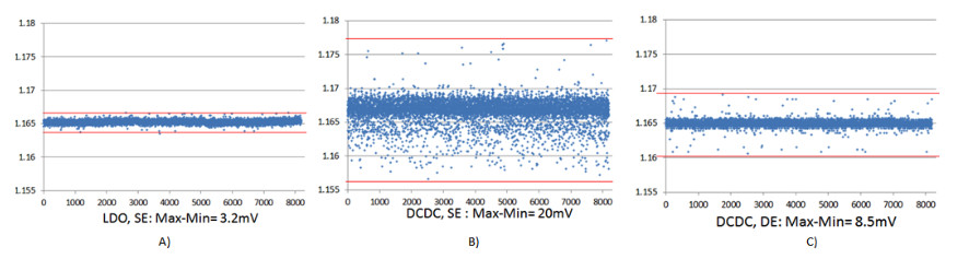
Comparing Figures 1b and 1c, if you make the same measurement with the DC/DC regulator in differential mode, the overall noise decreases and the difference between the LDO and DC/DC performance is minor. Figure 1 shows performance in volts instead of least significant bit (LSB), with the vertical axis converted to volts since the LSB of the differential is twice that of the single-ended to account for the support of signed results (negative voltages). The variance in the differential measurement is less than half the variance in the single-ended implementation, showing that the ADC sees the majority of noise from the DC/DC as common-mode noise.
The DC voltage being measured is treated as a differential input, where Vss is the negative input to the ADC. So even though the signal itself is a single-ended signal, measuring in differential mode enables a reduction in noise – and moreover reduces noise when using a DC/DC regulator. This is very good news, enabling engineers to take advantage of the benefits of the DC/DC while eliminating the associated noise.
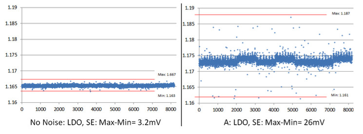
Noise from the internal regulator is only one possible source of noise. Other possible noise sources can be neighboring digital signals, such as I2C or Serial Peripheral Interface (SPI) communications, or a pulse-width modulated (PWM) waveform. We recommend keeping these signals as physically far as possible from the ADC pins – and if possible inactive during the ADC measurements. Most IC manufacturers intentionally keep digital signals away from the analog by creating dedicated analog pins. In smaller packages, however, some digital functions may be multiplexed with analog pins, or the digital input/output (I/O) pins can be neighboring to the analog pins.
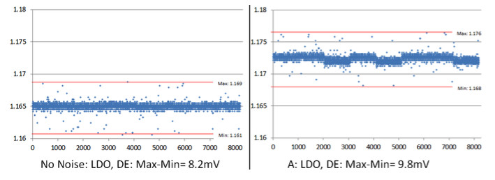
As an experiment, let’s locate the DUT analog input immediately next to a 48MHz clock output (full rail-to-rail swing) to represent a digital noise source. As shown in Figures 2 and 3, the increase in noise with the addition of the neighboring clock output is greater with the single-ended measurement compared to the differential. In the single-ended case, the voltage measured is connected to the analog input. What would be the complementary input in differential mode is left in general-purpose I/O (GPIO) mode and actively driven low, the device’s digital source supply voltage (DVSS). In the differential case, the complementary input is externally connected to the device’s analog source supply voltage (AVSS).
Although small when compared to the single-ended example, the differential result indicates that noise is still present. A visual inspection revealed that the clock is relatively close to the positive leg of the differential measurement when compared to the separation between the positive and negative legs of the differential pair. Therefore, the relative coupling will not be equal and the noise will not appear completely as common mode.
This experiment was conducted on a four-layer PCB, with the third layer providing an almost completely solid ground plane so that return currents may follow directly below the trace. The second layer provides reference voltages and is split in several places, complicating the coupling between the signal and ground plane return path and potentially creating a medium for noise to impact the measurement, which may further explain the presence of noise
In this last experiment, an evaluation module transmitting 100 random packets at 50kB (868MHz, 2GFSK, 2kHz deviation) introduces a radio signal. The EVM was placed adjacent to the DUT so that the MCU (and ADC) are approximately 6cm from the EVM’s PCB antenna. Figure 4 again shows that the differential configuration is superior in noise immunity over the single-ended. The key is that the energy couples uniformly on both the positive and negative inputs of the differential ADC, so the signal is rejected as common modeIdeally there would be no noise seen in the differential measurement shown in Figure 4, so this deviation from the expected merits discussion as to the potential reasons.
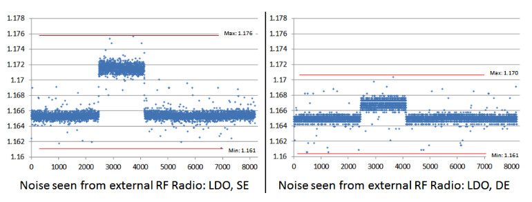
The most notable difference between the experiments with the clock and Sub-1 GHz radio is the relative coupling area. In the case of the clock, the coupling area was most related to where the clock trace ran parallel with the ADC input lines. After this parallel run, the signals diverged: the ADC signals went off-board to the voltage source for measuring, while the clock terminated at another receive input.
It is the off-board connection with minimal shielding that provides a potential way for radio energy to couple into the ADC. Moreover, any differences in electrical length between the positive and negative inputs to the ADC can cause the coupled noise to be differential rather than common mode. One powerful way to minimize differences in electrical length between the positive and negative inputs of the ADC is to design signal paths that are symmetrical.
The testing in this section was intended to show the breadth of improvement made available by differential signaling. The improvement occurs at an application or implementation level. Interference from a neighboring radio is also applicable to Bluetooth and Wi-Fi applications that need electromagnetic compatibility (EMC). Improvement was also evident at the board level, with cross-coupling (cross-talk) from a neighboring digital signal. And finally, improvement was even visible at the IC level, where choosing a noisy regulator achieves lower-power operation and mitigates the reduction in ADC performance.
While differential signaling can be an invaluable tool to achieve the ADC performance found in the data sheet, understanding the data-sheet parameters must be the priority. There are many configurations and dependencies within the MCU related to ADC performance, which can make comprehending data-sheet performance with respect to the application requirements difficult.
This series addressed some of the main performance dependencies and provided trends to help demystify the MCU data sheet and integrated ADC performance. Equipped with this understanding, a developer can make more informed MCU selections for sensor applications and implement a design that fully realizes the integrated ADC’s performance.