TIA Fundamentals Part 2: Signal Frequency Response
November 25, 2019
Story
Ultimately, at the end of the next three blogs, insights will be provided about the stability of the transimpedance amplifier (TIA) circuit.
In my previous blog on the DC transimpedance amplifier, The Fundamentals of Transimpedance Amplifiers, we began a good start towards understanding this simple circuit. Ultimately, at the end of the next three blogs, insights will be provided about the stability of the transimpedance amplifier (TIA) circuit. At this point, it’s time to get our hands dirty and dig into the AC response.
Start with the Core
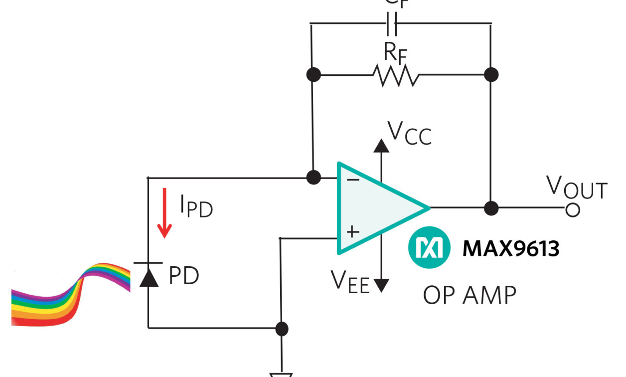
Figure 1 shows a standard high-precision TIA circuit with zero voltages across the photodiode (PD) using a low picoampere input bias current and a mV input offset voltage amplifier.
Figure 1. Standard high-precision
For precision, Figure 1’s amplifier has an ultra-low input bias current and offset voltage. To reduce current errors by being below the minimum IPD, the specified MAX9613 input bias current is 1pA (typ). To keep linearity as good as possible with the photodiode’s response, the MAX9613 offset voltage is an ultra-low 150mV (max).
With the surrounding actual and parasitic capacitances, this TIA has the potential to be unstable. But hopefully, with the new design expertise you will acquire from this blog series, you’ll be able to design out this unpleasant condition.
In Figure 1, the signal gain is equal to the combination of the feedback network and the parasitic resistance of the photodiode. The signal gain formula (Equation 1) is:
VOUT / IPD ≈ (RF || CF) Eq. 1
In Equation 1, if you assume CF is an open circuit the estimated DC gain of this transimpedance circuit is RF.
Further examination of Equation 1 renders a pole frequency (Equation 2) equaling:
ƒP = 1 / (2 p RF x CF) Eq. 2
The signal frequency response exhibits a DC response at RF and fP at a higher frequency (Figure 2).
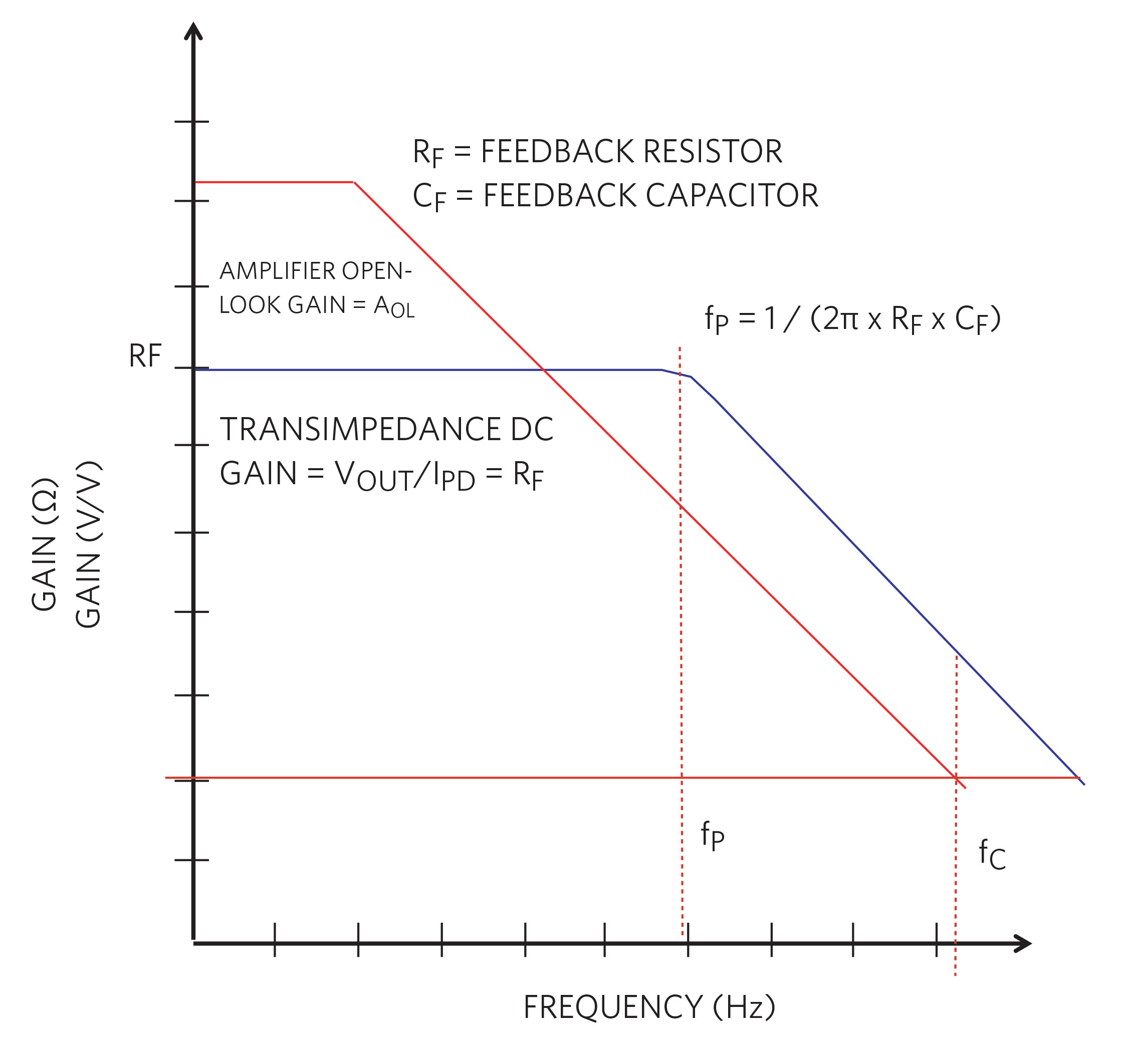
Figure 2. TIA signal frequency response.
In Figure 2, the signal is gained on the inverting side of the amplifier. The DC gain of the TIA is equal to VOUT/IPD. Conveniently, this gain is equal to the feedback resistor, RF. As frequency increases, the gain remains stable until the corner frequency hits, where RF and CF form a lowpass filter.
That’s the story of the TIA’s signal response, but we still have not talked about stability or circuit ringing in the AC domain. Figure 1 has two fundamental areas that we will use to further clarify the AC stability response:
1) Op amp circuit, which will include all the op amp parasitics.
2) Photodiode, with all the photodiode parasitics.
The components and parasitic capacitances and resistances in these two areas will frame out the step response characteristic. In our upcoming evaluation, we will find out how the amplifier and photodiode parasitic capacitances have a major impact on the circuit’s stability. See you in the next blog.