MEMS Packaging for High Volume Products
March 19, 2020
Story
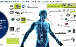
Micro Electro-Mechanical Systems, or MEMS, is an enabling technology. It merges the versatility of semiconductor technology with the functionality of mechanical structures.
Micro Electro-Mechanical Systems, or MEMS, is an enabling technology. It merges the versatility of semiconductor technology with the functionality of mechanical structures at a scale that opens entirely new application areas. MEMS technology enables smart phones to provide orientation, or fitness trackers to detect when we’re running, sitting or sleeping. But, MEMS technology can do so much more than just ‘sense.’ It can operate as an input to a system, or output (actuator) and integral part of a control or feedback loop.
For example, the demand for MEMS-based RF filters is expected to increase with the roll-out of 5G, because they can deliver higher performance in terms of insertion loss and the power they can handle. Analysts such as Yole Developpement SA expect the market for MEMS RF filters to grow at a much higher rate than the rest of the market (including sensors for consumer applications) over the period between 2018 to 2023.

Source: Yole Developpement
The technology refers to structures with features measuring between 1 and 100 micrometers (objects that are smaller than 1 micrometer are referred to as nano electro-mechanical systems, or nanotechnology).
The idea that objects of this scale can do any useful work, in a mechanical sense, may be difficult to accept, but many of the principals that underpin electronics have no issue with scaling down to this level. This includes capacitance, inductance, magnetism, and optics. When coupled with the ability to form movable objects, it becomes easier to conceive how a micromirror could deflect light in a communications device, or a variable capacitor could be adjusted in an RF filter.
Actuators formed from miniature motors can be exploited to physically adjust electronic components using magnetism, expansion, and even steam. Tiny Stirling engines have been manufactured in MEMS devices that perform physical work, using electricity to heat a fluid that expands within a piston, for example.
The fundamental manufacturing processes used to create MEMS devices are based on semiconductor manufacturing. This is not an accident. All semiconductors are manufactured using a combination of deposition and lithography. Most are considered planar devices. Their features (transistors) extend in the X and Y axes of a substrate. Some power devices, known as Trench transistors, extend someway into the Z axis. MEMS takes this concept two stages further, by creating 3D structures using the same processes of depositing a material selectively removing it, and then enabling those structures to physically move.
Sensors remain a huge part of the MEMS market and here the moving element is often a diaphragm, the movement of which modulates the resistive or capacitive properties of the material. In the case of a MEMS microphone, the movement would be caused by modulated sound waves, but the same principle is used in pressure sensors. Other types of environmental sensors, such as humidity and temperature, operate by detecting the changes in capacitance and/or resistance in a deposited material, due to the medium being measured.
Motion sensing has revolutionized consumer devices and it is also being applied to other verticals such as the automotive, medical, and industrial industries. In a MEMS device, motion is typically detected as the displacement of a mass, attached to the main substrate through small pillars or some other form of tether. The movement transferred to the substrate through these tethers results in a change in capacitance or resistance, which is measurable in the same was as described above.
Micromechanical machines comprise actuators, use transmissions, ratchets, and other forms of mechanical elements to turn small scale movement into useful work. Microfluidic actuators are now commonly used in inkjet printers to deposit small amounts of ink. Micropumps and microvalves are used to control nano- or pico-litre volumes. The same techniques are used to create the so-called ‘lab on a chip’ which are revolutionizing areas of biological study and analysis.
Taking MEMS to High Volume Production
The global MEMS market is predicted by analyst Allied Market Research to be worth in excess of $122 billion by 2026. This is thanks to a compound annual growth rate of 11.3% between 2019 and 2026. With an erosion in average selling price, the volume of MEMS devices that will ship in the coming years is clearly increasing significantly.
This increase is attributed to the influence of megatrends such as the IoT, wearable technology, smart consumables, and the emerging demand from autonomous vehicles and the automotive industry in general. Coupled with this, there is expected to be positive developments in the area of fabrication processes, leading to higher levels of reliability.
Packaging forms a key part of the manufacturing process. For majority of MEMS devices, including inertia, pressure and temperature sensors, the most common type of packaging is the cavity package. This provides the protection needed by the sensitive electro-mechanical substrate while maintaining physical space between the package and the substrate.
However, cavity packaging was originally developed in association with early MEMS activity, when the focus was on performance, rather than high volumes. As a result, not all cavity packaging for MEMS is cost-efficient for high volume manufacturing.
UTAC offers a cavity lid packaging technology that has been developed to support volume production. This includes being able to select the most appropriate materials for the application and the plating type used. The lid attach technology offered by UTAC supports metal, glass and plastic materials, as well as multi-die configurations. This extends to precise single and multi-die attach demands.
Because MEMS contain parts that must be free to physically move, their packaging must include free space. Their relatively fragile nature also puts them at a disadvantage in terms of the stresses regular semiconductor die can withstand during the packaging process and the materials used. For example, die coatings must be sensitive to the needs of MEMS, while still providing protection. Reducing the stress, a MEMS device is exposed to during backend assembly will increase yield and maximize its working life.
With demand from applications such as wearable devices, the need for smaller MEMS components is also increasing. The result is that the cavities inside the packaging, which can be thought of as controlled atmospheres, are also growing smaller. This puts even more emphasis on the need for high quality and reliable packaging technologies, with a focus on choosing a partner that can deliver a comprehensive approach to the package design, manufacture, assembly, and testing stages.
In addition to packaging finished die, UTAC is also able to offer a range of services for the preparation of MEMS devices. This includes processes such as wafer thinning, essential when shaping die in the backend assembly stage, wire bonding and compression molding for lower stress. Low stress materials for die attach and mold compounds are essential here and represents another area of expertise offered by UTAC.
Packaging Types for MEMS Devices
In low volume or niche applications, the choice of packaging format is less important than the way the device performs. However, by moving to standardized packaging outlines, manufacturers can expect higher yields and greater reliability in large volumes. This is the challenge that suppliers now face and an area where outsourced semiconductor assembly and test providers, or OSATs, like UTAC, are focusing significant efforts.
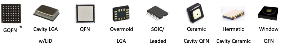
UTAC is able to provide MEMS packaging in standard formats, including GQFN, QFN, and SOIC. The same can be said for cavity LGA with lid, over-mold LGA, and ceramic cavity QFN. All of these package types are now being produced in high volumes, in various body sizes and wire types, and in different form-factors.
The R&D teams within UTAC have extensive experience of meeting customer requirements while complying with best practices to ensure high reliability. This is apparent by the wide array of MEMS devices UTAC is currently producing. The devices include oscillators, RF tuners, and sensors for detecting movement. Orientations such as magnetometers, accelerometers and gyroscopes, and environmental sensors including pressure and temperature are also included.
Source: UTAC Group
As MEMS solutions move into higher volumes, working with the right OSAT will become more important. UTAC offers a full service for MEMS packaging design, assembly and test, with the expertise and experience manufacturers are looking for when choosing a trusted OSAT partner.
Author Bio
Asif R. Chowdhury
Asif joined UTAC in March 2014 and heads the group's product line and marketing function. He has more than 20 years of experience in managing business units, business development, process engineering, design, research and development, and strategic sourcing in the semiconductor industry and related fields. Prior to joining UTAC, Asif was working with Analog Devices Inc. and based in Wilmington, Massachusetts where he was in charge of its MEMS package development and assembly engineering, and strategic sourcing for assembly and test.
Asif holds a Bachelor of Science in Mechanical Engineering from the University of Texas at Arlington and a Master of Science in Mechanical Engineering from Southern Methodist University. He also has a Master of Business Administration and Master of Science in Finance from Northeastern University.