Addressing EMC Preemptively in Ethernet Connected Devices
October 14, 2019
Product

Making sure devices are compliant with or meet the requirements of EMC, the process of keeping EMI under control so other nearby devices are not impacted, can be frustrating.
Introduction
Electromagnetic interference (EMI) is an issue every designer of Ethernet-connected devices has to deal with. Making sure the devices are compliant with or meet the requirements of electromagnetic compatibility (EMC), the process of keeping EMI under control so other nearby devices are not impacted, can be frustrating.
While simulation modeling and other design tools will help achieve 90 percent of EMC goals, the following additional steps are required to complete the final 10 percent.
- Complete the printed circuit board (PCB) layout.
- Components are fully populated on the PCB and assembled, usually by an automated machine. The assembled circuit board is referred to as the printed wired board (PWB).
- The PWB is placed in an EMC chamber to test for electromagnetic radiation. If excess radiation is detected, PCB layout must be repeated.
Engineers and developers can find themselves attempting to design an EMC-compliant device with incomplete knowledge of how to identify EMI sources. In addition, EMC compliance testing typically occurs late in the development schedule when the product is in verification testing. If there is a problem, engineers will need to redesign, layout the product again, and retest. The necessity to repeat these steps means that EMC compliance failures will slow the schedule and bump project costs up.
The article will provide guidelines on PCB layout, discussing a preemptive approach to solving EMC problems and shortening the PCB design cycle.
PCB Design and Layout can be Time-Consuming
Despite the available tools and design experience, it is difficult to achieve 100 percent EMC compliance in the first design pass. Because it is too time-consuming to model, predict and address this problem, the traditional approach has been to build the best evaluation unit possible and make corrections for the next iteration.
Another strategy is to create a flexible design that requires minimal redesign. For example, IC design engineers consider every aspect of die layout, routing and device placement to maximize silicon utilization. They also pack spare devices into the blank areas of the die just in case. During fabrication, the engineers hold wafers at the intermediate steps so that they can make revisions without delaying the production cycle. As a result, the redesign cycle time is greatly reduced.
PCB designers can adopt a similar strategy.
The PWB layout is critical to the success of the product design. However, it rarely receives the attention it deserves, particularly in the context of EMI mitigation in high-speed digital and analog signals. So, it is crucial to understand the layout guidelines for PCB design, shown below, as they pertain to EMI and signal integrity.
PCB Layout Design Rules
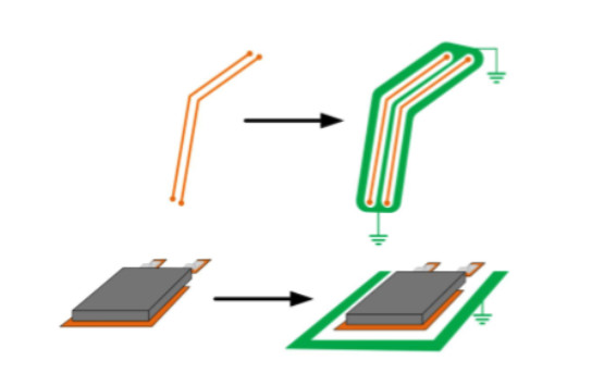
- Decreasing the Loop Area and Antenna
The source and return path of any signal form a circuit, which creates a loop antenna. The strength of the radiated signal is proportional to the loop area, the current flowing through it, the length of the signal path, the frequency of the signal, and the impedances of the source and loop. Furthermore, the direction of the radiated signal depends on the loop path length compared to signal wavelength.
Both the loop length and area need to be minimized to mitigate EMI. If this is not possible, then the EMI needs to be shielded. However, incomplete shielding can result in the creation of a ground plane reflector, which may enhance radiated emissions in the unshielded direction.
- Reducing Parasitic Capacitance
Loop antenna paths can form in the common mode (CM) signal path with earth ground. All AC signals capacitively couple to their surroundings. Current flows through the parasitic capacitance and finds a return path, which forms the loop antenna. Even though the capacitance is small and the currents tiny, the loops can be very large.
Since it is impossible to eliminate parasitic capacitance, the strategy is to shorten the signal path. Appropriately rated capacitors can be placed between the primary and secondary circuit grounds and as close as possible to the transformer. With a clever PCB design, capacitance can be created using overlapping primary and secondary ground planes on separate layers of the PCB.
- Connecting Earth Ground and Signal Ground
Typically, earth ground and signal ground are connected to reduce loop size. But systems that require source isolation, such as AC mains-powered applications, do not allow the direct connection between the primary signal ground to the earth ground. Instead, the secondary signal ground may be connected to earth ground to minimize the common mode circuit path. In this scheme, most of the current will flow through the intended path without eliminating parallel paths. A series impedance, such as common mode inductors, must be added to block undesired current paths. An example is the conducted CM EMI filter found in power supplies. The CM inductor impedes CM current flow toward the power source, and the capacitors to ground provide a shunt return path.
- Balancing Differential Pairs
Another common mode current source is differential-to-common mode conversion in unbalanced differential pairs. Ethernet signals are transmitted over twisted pairs in the cable and converted to a microstrip or stripline transmission line on the PCB.
If the series and shunt impedances are not identical in both signal paths, a common mode current will flow. Unequal parasitic capacitance to ground may cause impedance mismatch.
- Minimize the Impact of PCB Design on Signal Integrity
The PCB design may affect signal integrity by causing insertion loss, return loss and crosstalk. The insertion loss is the attenuation of power between the source and the load. Return loss measures the portion of the transmitted signal that is reflected from the source. Lastly, the coupling of adjacent signals is the cause of crosstalk.
It is essential to maintain the characteristic impedance with a low-loss transmission line to minimize the impact of radiated emissions on signal integrity. Also, it is important to space the adjacent differential pairs adequately.
- Watching out for Other Single Discontinuities
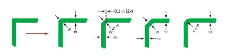
An ideal layout of signal traces would route the differential signals from the source to the load using the shortest equidistant straight-line path on one PCB layer. While single discontinuities such as sharp corners, vias, and changes in ground plane coupling make little difference, cumulatively, they have a significant impact.
A sharp trace corner creates shunt capacitance to the ground plane, which degrades insertion loss. On the other hand, the sharp trace corner increases the local E-field strength and radiated emissions. Therefore, trace corners should be round with a radius no tighter than the differential pair separation.
Vertical interconnect access () introduces discontinuities that impact the characteristic impedance. Any discontinuity will degrade the insertion and return loss. Vias create both inductance and capacitance, with inductance having the greater signal integrity impact. Capacitance is formed between the annular rings surrounding the via and internal ground plane(s). Minimizing the diameter of the annular rings and maximizing the diameter of the plane void (anti-pad) reduces capacitance.
If smooth curves are not possible at trace corners, then engineers should aim to create trace corners with cumulative turns of no more than 45 degrees. If the inside corner needs to be at a sharper angle, then the outside corner should be rounded.
If the designer cannot avoid vias, then he must take care to maintain the characteristic impedance when the signal path transitions to another PCB layer. Characteristic impedance depends on the geometry of the traces and their relation to each other, the plane(s), and nearby signal traces. While it is possible to compensate for the changes in characteristic impedances, it is much simpler to put a priority on the routing of the signals so that layer changes are unnecessary.
- Designing Signal Return Path
The signal return path is often overlooked during PCB design.
Most designers create interconnected ground planes without considering vias or signal routing on the ground plane. Vias and signal routing will interrupt the current flow and cause the return current to follow the lowest impedance path back to the source.
For DC and low-frequency signals, the lowest impedance path is dominated by resistance, and the current follows the shortest distance. For higher frequencies, the impedance is dominated by inductance. As the frequency of the signal increases, the signal edges will become noisy and degrade circuit performance.
Due to cost considerations, engineers often have to put mixed signal types on a common plane. They not only have to separate grounds into digital, analog and power, but also minimize the impact of parasitic elements on adjacent circuitries of the same category.
Crosstalk also compromises signal integrity. Capacitive coupling can be reduced by crossing at a 90-degree angle or separating traces, which overlap or are parallel to each other. Crosstalk may be further minimized by using guard rings. Guard rings are also useful in reducing inductive coupling.
- Designing Trace-to-Trace Separation
Trace-to-trace separation is also overlooked in PCB design.
Most designers are familiar with worldwide safety agency standards (UL, IEC, for example), which primarily address electrical hazards and flammability. However, these standards do not address reliability.
A voltage potential between traces can cause metallic whiskers (dendrite) to grow over months or years. Eventually, the dendrite will short the traces and lead to product failure. PCB design standard IPC-2221, ‘Generic Standard on Printed Board Design,’ defines trace spacing requirements to avoid electromigration. Engineers should try to design the trace-to-trace distance to be above the IPC-2221 guidelines.
Taking the Preemptive Design Approach with Filtering
After all the PCB design guidelines described above have been observed, now it is time to apply the design strategy to include passive and active filtering to solve the EMI problem preemptively. Here are the pros and cons of each approach.
Passive EMI filtering
To minimize the impact of differential to common mode current conversion in the Ethernet interface design, a small CM inductor, commonly known as balun, can be added. The transformer action (assuming a coupling coefficient of 1.00 and ignoring magnetizing current), of the CM inductor will force the currents in each line of the differential pair to be equal and opposite. The CM impedance is very high, and the differential impedance is (ideally) zero. To implement such a solution, the CM inductor is placed as part of the layout. Upon the final test, if it is not needed, it can be removed from the bill of materials (BOM) and replaced with a jumper.
However, a passive filter solution can cause performance to degrade in some applications. The degradation occurs because CM inductors do not have an ideal zero differential impedance, so there is an introduction of insertion loss and characteristic impedance.
Active EMI Filtering
Alternatively, active filtering can be implemented to solve the EMI problem. During the final test cycle, if the PWB design already meets EMC, then there is no need to install the active filter. Otherwise, include the active components in the PWB. This can be done by creating a placeholder on the PCB and calling this out in the BOM as an option.
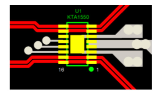
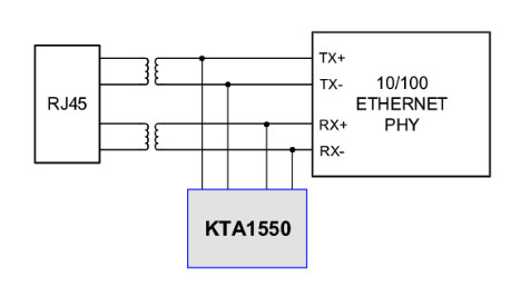
Here is how active filtering works. As shown in Figure 3, either the dual-channel (KTA1550) or the quad-channel (KTA1552) active EMI and electrostatic discharge (ESD) suppressor IC from Kinetic for Ethernet applications can be routed through the data lines as a contingency. The IC is located between the PHY and the LAN transformer.
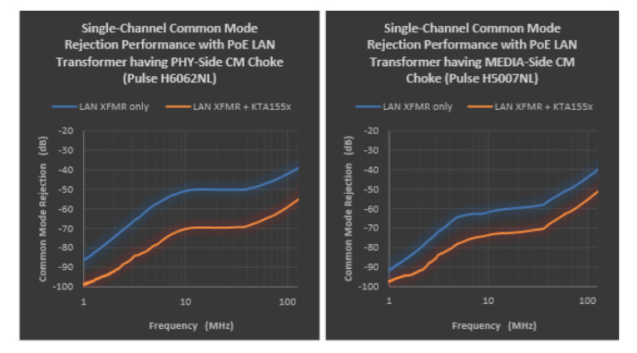
The KTA1550 supports two twisted pairs (Figure 4) while the KTA1552 supports four. Active filtering reduces the noise level via common mode rejection. If passive filtering is already installed, the add-on active filtering functions can achieve additional noise reduction.
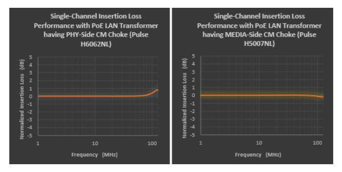
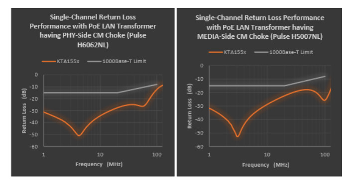
Using active filtering can reduce CM emissions by up to 10 dB from 1 to 125 MHz with almost no impact to insertion, return loss, or characteristic impedance compared with the passive-only approach. Both ICs are compatible with voltage and current mode PHYs. Operating in the industrial temperature range from -40 °C to +85 °C, the device consumes 180mW with a single standard power rail (3.3V or 2.5V).
Common applications of active filters include Ethernet systems requiring additional CM suppression to meet EMC Class B emissions or higher EMI immunity requirements and ESD protection, PoE and non-PoE Ethernet systems, VoIP phones, IP cameras, and other network installations.
An active filter IC will have higher BOM costs than a passive balun, but the active filter IC is more successful at lowering noise, as Figures 5 through 7 indicate. The benefits of using an active filter can be summarized as follows:
- Higher common mode rejection can be achieved than using passive filtering alone.
- No insertion loss or introduction of characteristic impedance compared with passive filtering.
- Additional ESD suppression will come from the active filter IC.
Summary
Electromagnetic interference is a serious issue in printed wiring boards (PWB). Therefore, the reduction of EMI-induced noise is a significant challenge in PCB design.
Engineers often get trapped in a whack-a-mole scenario, where they have to keep adjusting the design to address new problems that arise from attempts to solve old issues. As a result, the PCB design has to undergo many rounds of redesign and re-testing, causing production delays and incurring extra development costs.
Active filters can help engineers solve this conundrum by achieving complete noise suppression without creating new noise-related issues. Furthermore, active filters fit easily into PCB designs and are equally easy to install. Therefore, they provide a significant return on investment, reducing design and production delays, and minimizing costs.
For more details on PCB design rules, download the white paper here.
Phil Dewsbury is the Senior Director of Product Marketing at Kinetic Technologies. Dewsbury has experiences in marketing, sales and technologies. In product management and planning, he predicts industry trends to develop new products to meet future market demands.