Smart Home ? One chip Graphics, Touch, and Wireless Solution! - Part 2
November 24, 2020
Story

In part 1, we covered the general Smart Home market trends, user interface, and sensing requirements. In this part, we will cover connectivity and security requirements for Smart home applications.
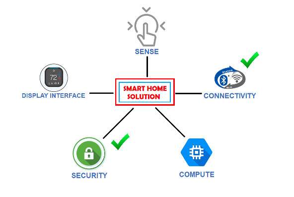
In part 1, we covered the general Smart Home market trends, user interface, and sensing requirements. In this part, we will cover connectivity and security requirements for Smart home applications, including the requirements shown in Figure 1.
Figure 1: Requirements of a Smart Home System
Connectivity
Move out of a room, lights turn off automatically; the door camera detects a parcel, it sends a notification instantly; out of groceries, the refrigerator places an order for you. The wow factors! That is what connectivity is about. All the magic you see that gadgets perform depend upon connectivity. Connectivity between devices and to cloud is a must for a smart home device. The mode of connection may be wired or wireless. Wireless is the widely used mode for its obvious advantages.
LPWAN, Cellular, Zigbee, Bluetooth, Wi-Fi, and RFID covers most of the wireless technologies for smart home applications. Wi-Fi and Bluetooth are the widely adopted or de facto connectivity choices in smart home devices because of their versatility in bandwidth, throughput, range, and power consumption. Bluetooth is used for low bandwidth, short range, and low power applications. Wi-Fi, on the other hand, is used for high bandwidth and long-range applications requiring Internet connectivity. In a system, Bluetooth and Wi-Fi can co-exist to overcome the disadvantages of the other (for Example CYW43012) Battery operated devices in the household use Bluetooth as a medium to talk to each other, a Bluetooth to Wi-Fi bridge then gives those devices the ability to connect to internet. Many MCUs integrate wireless connectivity as part of their SIP packages. This not only saves cost, but also the area the chips occupy. In addition, it physically secures the communication channel between the MCU and connectivity chips.
An example of a WiFi Connectivity implementation in the Smart Home
Consider a use case where there are multiple sensors monitoring humidity, temperature, soil moisture, etc. across the home. Multiple controllers such as thermostats, humidifiers, and plant water controller use the data from these sensors. These sensors and controllers within the house can use Bluetooth or Bluetooth Low Energy (BLE) connectivity for communicating with each other and a user smartphone or a unified controller running Google Home or Amazon Alexa. This controller would in turn connect the sensor network to internet enabling remote control and monitoring. While the sensors located in a room may be power-constrained, these controllers typically have access to wall-supply. This would determine the type of devices we select for each device in the smart home environment. Sensors require an ultra-low power BLE controller such as the PSoC 6 BLE, whereas controllers can include SIPs with MCU, WiFi, and BT in a single package such as CYW9P62S1-43012EVB-01 SIP packages for providing additional processing and functionalities demanded by the controller application.
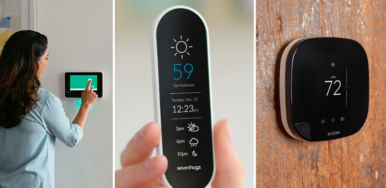
Libraries and RTOS environments make it easier to schedule tasks on priority, making a single MCU handle and coordinate all the operations. A device with a display, touch sensing, and wireless connectivity can fall in a wide range of smart home applications. Smart thermostat, smart coffee machine, smart refrigerators, etc., are prime examples.
Figure 2: Some smart home devices
Security
All the features we’ve discussed only make the device smart. With the versatility of connectivity, comes the disadvantage of security threats. Security threats can range from simple data theft to malicious firmware or application execution that could compromise the whole system and in turn the house. Thus, the device and its execution environment must be secure as well.
First and foremost, in security, the primary focus is to ensure the communication network is secure. For a secure network, the underlying communications chip should have WPA and WPA2 (Personal) support for powerful encryption and authentication in addition to AES in WLAN hardware for faster data encryption and IEEE 802.11i compatibility. Devices using Bluetooth Low Energy should have secure connections supported in hardware for the highest level of Bluetooth network security. Along with these network security backbones, additional security features like certificates should be used to authenticate the device/server a smart system is talking to. Many IoT MCUs provide hardware based encrypted data logging to external storage for additional secure storage.
Over-the-air (OTA) updates forms one more class of security enhancers. It helps with applying important security patches to the running application and even to the wireless host/controller firmware. OTA also introduces new features and allows devices to be more relevant in the market. Secure storage, secure operation, and secure communication should be the guideline for any smart home-based application.
The first and foremost requirement for any application that has upgradeable firmware is to ensure it is running authentic firmware from the intended source. In addition, depending on the security requirements, the upgrade or patch needs to be encrypted as well. These authentication and encryption procedures should themselves be tamper proof. This requires a root-of-trust flow from boot in the MCU hardware like booting the MCU with non-programmable code with tamper-proof hardcoded keys. This would ensure the encryption and authentication procedures performed by the boot code using the keys can always be trusted.
Once the root-of-trust is established, the level of security offered by the authentication and encryption procedures come into play. Public-private key algorithms such as RSA or Elliptic Curve algorithms combined with SHA can be used for a secure authentication and AES algorithms can be used for encryption. As with any encryption algorithm, the keys are very important and need to be secured/stored safely. MCUs need integrated hardware support to provide a root-of-trust and protect keys. The PSoC 64, for example, integrates security with connectivity, processing, and peripherals. It employs a dual-core approach with a secure M0+ core running the trusted environment and handling all secure executions while a non-secure M4 core runs the authenticated user application for the smart home system.
While it is important to execute authenticated code in the device, it is also important to secure the connection with external memories that store this information. The information may not be sensitive in all cases. However, for those applications storing sensitive information such as sensor data logs, firmware update patches, and even code that executes out of the external memory, an encryption mechanism over the memory interface would be preferred. MCUs offering on-the-fly encryption and decryption are considered an added advantage. This encryption mechanism ensures the data stored in the external memory is safe even if a hacker gets his hands on the hardware. An on-the-fly encryption/decryption mechanism would be preferred for code execution out of external memory. For example, PSoC 6 device family offers both an on-the-fly AES encryption/decryption mechanism over the Quad-SPI memory interface along with a separate dedicated Crypto HW for advanced encryption/decryption options.
Integrated Solution (Graphics, Touch, Sense, and Wireless System):
The individual features we’ve discussed so far make a smart home device very appealing to the market. All these features work well when used individually but integrating them to work together requires lot of design attention. The biggest challenge is to build a system that provides optimal performance along with system security without increasing the overall system cost. All MCUs have limited flash, limited memory, limited peripherals, and limited CPU time to perform any operation. When designing such a complex system, allocation of these limited resources determines the final performance of the smart gadget.
Challenges in building an integrated solution:
1. Integration
The first challenge would be to integrate all the features into the application. By using different chips for individual features such as WiFi connectivity, MCU processing, User Interface etc., there is a need for additional space for individual chips and their components, communication overhead between chips, and different development platform overhead impacting time-to-market. It would be worth investigating solutions/chips that offer integration of various features – this reduces cost and time-to-market. Devices like the CYW9P62S1-43012EVB-01 are a good example for building an integrated architecture for an IoT application.
2. Performance
The next challenge would be to meet the performance requirement along with integration. Performance requirements can vary from connectivity performance to user interface responsiveness. This is where the value of integration needs to be weighed in. As you integrate more into a single chip, the performance side of the system starts taking a hit. In order to meet performance requirements at the same time enjoying integration requires a multi-core chip architecture, where each core takes care of an individual feature such as WiFi connectivity related processing, general application processing, security, and UI processing etc.
In a real-world scenario, all the features do not need to run at their peak performance simultaneously. For example, there is no need to allocate resources to process the user interface when there is no one attempting to interact with the device. The necessary background data can be processed beforehand at an idle time and tasks can be offloaded during usage. This is where proximity and other sensors come in handy: the data from these sensors can be processed to allocate resources to tasks that are required only at that moment. For example, touch processing can be started only on a proximity or touch detection (ganging sensors). The resources available are as good as the designer allocating them. By carefully analyzing the need of the system at different moments and allocating resources only when needed are the key factors to obtain peak system performance.
3. Security
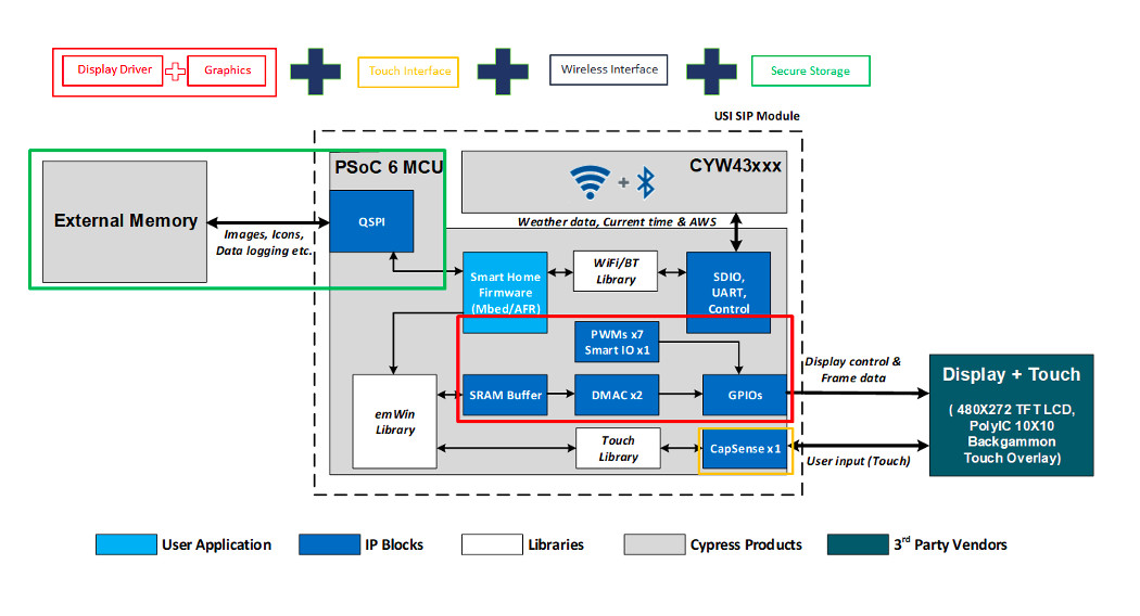
Finally, with smart home and IoT becoming the future of technology, the need for secure implementations is on the rise. One added advantage of integrated architecture is the limited scope for hardware probing of peripherals that would otherwise be impossible in multi-chip implementations. In addition, ensuring a secure operating environment for the application would be key to meet and overcome this challenge. An implementation example using PSoC 6and CYW43012 into single package CYW9P62S1-43012 is shown in Figure 3 .
Figure 3: A Implementation Example
In upcoming part(s), we will be covering more integration components and examples; stay tuned!
Jaya Bindra works as a Sr Manager Applications Engr at Cypress Semiconductor Corporation where she is managing the Embedded Applications Group and Solutions Development using the PSoC and WiFi/BT platform. She has 15+ years of experience in the Semiconductor Industry. She earned her MBA credential from IIM, Bangalore and holds a bachelor’s degree in Electronics Engineering from the Kurukshetra University. Jaya can be reached at [email protected].
Yeshwanth KT is an Applications Engineer at Cypress Semiconductor Corporation. He works on embedded application development with Cypress’ PSoC platform. He has 2+ years’ experience in Embedded System and Solution development. He holds a bachelor’s degree in Electronics and Communication Engineering from SJCE Mysuru. Yeshwanth can be reached at [email protected].
Meenakshi Sundaram is a Principal Applications Engineer at Cypress Semiconductor Corporation. He works on Bluetooth low energy and System-on-Chip solution development with Cypress’ PSoC platform. He has 9+ years’ experience in Embedded System and Solution development. He holds a BS degree in Electronics and Communication Engineering from Anna University. He can be reached at [email protected].