
Producing and verifying quality FPGA IP
May 01, 2010
Story

Verification strategies can meet time-to-market needs for FPGA IP by preventing issues that can slow down a delivered core.
There is more to verifying IP than functionality. Interaction of features, variability in timing, and testing strategies all factor into a broader verification strategy.
FPGAs have evolved in the past decade, becoming larger and more complex. The Intellectual Property (IP) developed for FPGAs has likewise increased in size and complexity. To deal with this increased complexity, IP developers have embraced best-in-class verification methodologies. Even when using these methodologies, developing IP for FPGAs still poses unique challenges that the typical ASIC designer might not encounter.
FPGA development presents three key challenges. One is that FPGA IP is often highly parameterized, which can create a very large number of design variations to test. Another issue is that FPGA IP developers need to verify that timing can be met once integrated into the user design. Finally, the IP developed for FPGAs is more susceptible to architectural changes than IP developed for other platforms. It is important that the verification environment accommodate these architectural changes with a minimal amount of work as quickly as possible.
Parameterize features
An FPGA has a higher cost per gate than a corresponding ASIC, so designers targeting an FPGA are motivated to create IP that does not consume any more resources than necessary. Whereas the ASIC will implement all supported features, the FPGA has the option of implementing only the features that the customer needs. Therefore, FPGA IP can and should be parameterized so that synthesis will remove unwanted logic. As an example, the size of the Xilinx 10 GbE MAC core shrinks by about 25 percent if the Ethernet Statistics Gathering feature is not needed, freeing up FPGA resources for other logic.
When scoping out what will be parameterized, factors like data bus width, number of pipeline stages, and optional functionality are good candidates to consider because they permit the designer or customer to make trade-offs between performance and resources consumed. Further trade-offs can be made by parameterizing platform-specific features like Block RAM and DSP blocks, as opposed to using fabric logic.
The downside is that every added parameter creates another permutation that must be tested. How does the verification engineer know the parameter has been exercised for all values? The best way to do that is through gathering coverage statistics and analyzing the coverage reports produced by the simulator. For instance, if a design has a Data Width (DW) parameter that controls whether the IP uses a 32-bit or a 64-bit data path and a Pipeline (PL) parameter that controls whether it uses extra pipelining to help meet timing, a basic coverage report with simple cover points might show that both values of DW and PL were exercised. However, it would not show if a 64-bit data path was tested with no extra pipelining. To achieve that, SystemVerilog “crosses” and/or more complex cover points are used to report if a particular combination of parameters has been hit.
For a large set of parameters, it quickly becomes apparent that hitting every permutation will take forever if every parameter is allowed to be randomly set. The verification engineer has to define the subset of parameter permutations that are relevant and heavily weight those that are more likely to be used by end customers. Additionally, permutations that better exercise the design should be chosen, such as those that induce full FIFO conditions or rarely used state transitions. Constrained random verification is ideal for this purpose because it allows the tool to randomize parameter values according to the verifier’s constraints and uses coverage metrics to see if important permutations are being hit. If they are not, then the verifier can either run more tests or change the weighting of the constraint’s distribution of values.
Verify timing
One of the challenges FPGA IP developers face is ensuring that the IP can meet timing once integrated into the customer design. Because it is difficult to functionally verify designs with a large parameter space, it is similarly difficult to understand the effects of the parameters on the ability to meet timing. Another hurdle for the developer is that the IP might compete for FPGA fabric resources with other portions of the user’s design, which can make it more difficult to meet timing.
Developers can employ multiple techniques to help ensure the IP will continue to meet timing even when integrated into the user’s design. A representative example design is nice to have, but not necessary. If an example design is not available, double-register all I/O that will go to the FPGA fabric. I/O that go on or off of the chip should be connected to the appropriate locations.
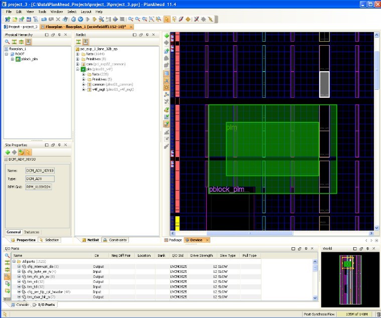
Once the design is in place, the next step is to implement the design in the targeted FPGA architecture. As part of the testing process, overconstrain the IP clock frequencies by 15 percent. Also, add an area constraint to the IP so that it is constrained to a region of the FPGA fabric that is not much larger than its minimal needs for placement, as shown in Figure 1. This will emulate congestion for when the IP is integrated into the user design.
|
|
The final step is to ensure that different parameter settings do not have an adverse effect on the ability to meet timing. Identify key parameters that are most likely to have an impact on timing closure. Randomize the identified parameters, run with the area constraint and higher clock frequencies, and ensure timing can still be met in all of the FPGA devices that the IP targets. The more combinations of parameters that developers run, the greater their confidence will be that the IP will meet timing in even the most difficult customer environments.
Decouple test scenarios from implementation
A designer might need to change the latency or data path width of the core late in the design cycle, either as a response to place and route indicating that the design will have difficulty meeting timing, or to take advantage of an FPGA that is faster and/or has a different number of resources. If the verification engineer did not anticipate that kind of change (for example, the test scenario assumed a fixed latency), then a large number of tests might need to be changed to code the new expectation. A well-designed verification environment will need few if any changes to respond to this.
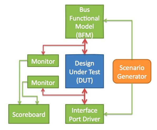
One of the best methods to decouple the test bench environment from the Device Under Test (DUT) implementation specifics is to use a scoreboard, as depicted in Figure 2. The test scenario pushes the expected results (for instance, packets) into the scoreboard, and as the DUT produces the data, it is compared to the scoreboard version automatically by the test bench. The test scenario does not need to be concerned when the DUT produces the data, only what data it produced.
|
|
Additionally, if the width of the data path changed and the data produced by the DUT is divided over several additional cycles (or unified into fewer cycles), then the scoreboard provides a single point in the test bench wherein the comparison to that expectation can be changed. The alternative of hard-coding the expectation in the test scenario requires that each scenario be updated when the DUT’s data width or data format changes.
Port drivers and monitors need to be coded to anticipate interface changes. An up-front effort that allows these modules to connect to ports and interfaces of different data widths can pay off later in the design and verification cycle when quick adaptations are needed.
FPGA IP, verified
The amount of IP available for FPGAs has increased tremendously during the past several years. To be competitive, vendors must consistently meet expectations for quality. Because time-to-market needs for FPGA IP are becoming more aggressive, vendors must do everything possible to prevent a delivered core from having issues that can slow down its customers. This means that well-thought-out verification strategies that can adapt quickly are a must.
Jason Lawley is a staff engineering manager in the IP Solutions Division at Xilinx, where he is currently managing Xilinx’s PCI Express solution. He has more than 10 years of experience designing and delivering IP targeted for FPGAs. Jason holds a BSEE from Cal Poly San Luis Obispo.
Jeremy Goolsby is a staff engineer in the IP Solutions Division at Xilinx. He has 12 years of experience designing FPGA IP and holds a BSEE from the University of Illinois and an ME from the University of Colorado.
Xilinx
408-559-7778
[email protected]
[email protected]
www.xilinx.com


