
Overcoming SoC design challenges moving to PCIe Gen3
June 01, 2010

With the new 128b/130b encoding scheme and scrambling polynomial, PCIe Gen3 presents a number of transmission and receiving issues, all of which are a...
The PCI-SIG work group intended to release versions of PCI Express (PCIe) that doubled the signaling rate with each generation. Starting with Gen1, the signaling rate of 2.5 GT/s doubled to 5 GT/s in Gen2, and was originally planned to double to 10 GT/s in Gen3. Encoding in the PCIe Gen1 and Gen2 protocols requires 20 percent overhead, thus making the effective data link rate 2 GT/s and 4 GT/s, respectively.
The group identified two choices for Gen3: Increase the signaling rate to 10 GT/s, keeping the same 20 percent overhead for the protocol, or specify a lower signaling rate of 8 GT/s with a lower encoding overhead. After six months of analyzing the technical feasibility of scaling PCIe interconnect bandwidth, the group determined that 8 GT/s could be manufactured in mainstream silicon process technology. They also determined that PCIe could be deployed with existing low-cost materials and infrastructure while maintaining full compatibility to the PCIe stack.
By enhancing the coding requirement from 8b/10b to 128b/130b, the new protocol reduces encoding overhead to 1-2 percent. As a result, PCIe Gen3 provides an effective link rate of 7.99 GT/s, thereby doubling the effective link rate from PCIe Gen2. The change in encoding schemes also includes a scrambling/descrambling algorithm as follows: x23 + x21 + x16 + x8 + x5 + x2 + 1.
PHY implementation challenges: transmit, receive
Jitter impedes the integrity of most communications links. This is even more pronounced in the case of high data rate communications. To effectively handle these challenges, engineers need to minimize the jitter generated and maximize the jitter tolerance. During transmission, clock generation in the form of a phase locked loop needs to generate as little noise and jitter as possible.
To do so, some designers implement a ring oscillator, while others choose an inductor capacitor (LC) oscillator. The ring oscillator generates more jitter, but it is still manageable in a 5 GT/s PCIe Gen2 PHY. However, for Gen3 at 8 GT/s, the LC oscillator’s lower jitter, which specifically lowers random jitter, helps reduce the bit error rate to better than the required 10-12.
PCIe Gen3 also incorporates an optional Spread Spectrum Clock Generation (SSCG) to reduce the spectral density of the Electromagnetic Interference (EMI). Without SSCG, PCIe Gen3 would radiate EMI on a number of narrow bands spread on the clock frequency and its harmonics. This results in a frequency spectrum that, at certain frequencies, can exceed FCC and other regulatory limits (JEITA in Japan and the IEC in Europe) for EMI. For this reason, some manufacturers use SSCG to implement PCIe Gen3 in consumer products and still meet EMI regulatory requirements.
Both transmission de-emphasis and reception equalization are required for PCIe Gen3’s maximum loss channels. As the data rate increases to 8 GT/s, onboard data losses increase because the transmission lines act as a low-pass filter and attenuate higher-frequency transmissions. The result: data looks corrupted. Gen3 recommends transmitter de-emphasis to boost high-end frequencies and de-emphasize low frequencies. In Gen3, de-emphasis has increased to 7.5 dB with a minimum rise time of 19 ps, as compared to Gen2 specifications of 6.5 dB with a minimum rise time of 30 ps. A three-tap feed forward equalizer is recommended for a PCIe Gen3 transmitter.
At the receiver, the transmission needs to recover from as much jitter and noise as possible. Different PHY implementations utilize different equalization schemes. Some use Continuous Time Linear Equalization (CTLE), which has proven adequate for 5 GT/s transmission. However, in addition to CTLE, 8 GT/s transmission requires another stage on the receiving side, Decision Feedback Equalization (DFE). When properly balanced, the two schemes minimize power consumption compared to relying completely on DFE. This balanced two-stage approach results in an open eye with the lowest possible power consumption.
A DFE implementation with a lower number of taps results in lower power dissipation. By conducting extensive system analyses with the requisite channel models and the balanced CTLE-DFE, designers can optimize the number of taps used in the DFE. MoSys’s PHY implementation has already validated this architecture in 10 GT/s SERDES silicon.
Controller-PHY interoperation
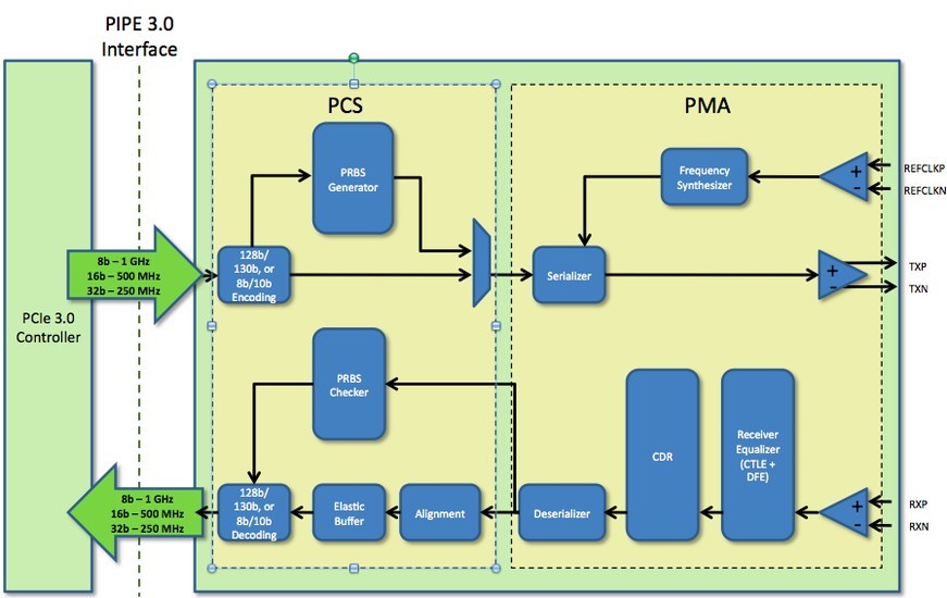
A System-on-Chip (SoC) design integrating a PCIe Gen3 link has to deal with both the controller (also known as the MAC or link layer) and the PHY, shown in Figure 1. The controller interfaces to the rest of the SoC through an on-chip bus on the one hand and to the PHY on the other. The interface to the PHY is explicitly defined by the PHY Interface for PCI Express (PIPE) specification. Thus, as a starting point, both the controller and the PHY must adhere to the PIPE specification to maintain compliance and ensure interoperability.
|
|
Additional key points
PCIe Gen3 requires several other relevant implementations, including three different breakout channels at 3 dB, 12 dB, and 20 dB; differential output voltage of 800 mV to 1,200 mV with a low-power option of 400 mV; and AC coupling and nominal 100 ohms differential termination. The differential return loss at DC and Nyquist frequency is 10 dB and 15 dB, respectively.
MoSys’ implementation of PCIe Gen3 IP blocks meets all of the requirements currently published in v0.71 and delivers the Physical Medium Attachment (PMA) solution in GDSII files and the Physical Coding Sublayer (PCS) as synthesizable Verilog register transfer level.
IP ready now
With the new 128b/130b encoding scheme and scrambling polynomial, PCIe Gen3 presents a number of transmission and receiving issues, all of which are addressed in the latest specification. MoSys has integrated PCIe Gen3 capabilities in currently available electrically compliant IP blocks, enabling SoC design teams to continue the design process and leverage the higher 8 GT/s speeds in new products. Per the specification, these blocks are backward-compatible with the 2.5 GT/s and 5 GT/s speeds of earlier generations of the specification.
Ali Burney is the director of SERDES and high-speed I/O products for MoSys, Inc. Prior to joining MoSys, Ali served as the senior strategic marketing manager for Achronix Semiconductor, where he developed the roadmap for next-generation products in the networking, wireless, and high-performance computing markets. He also spent eight years with Altera Corporation working as a technical staff engineer, system architect, and field applications engineer. Ali received his BSEE and MSEE from the Georgia Institute of Technology.
Prasad Saggurti is senior director of interconnects and embedded memory products at MoSys. He has more than 15 years of experience across varied product lines and industries, and was instrumental in designing leading-edge microprocessors at Sun Microsystems, digital audio and video CD chips at C-Cube, and DVD decoders at Mediamatics. He also managed semiconductor IP lines at ARM and Artisan Components. Prasad has an MSEE from the University of Wisconsin-Madison and an MBA from the University of California-Berkeley.
MoSys
408-731-1800
www.mosys.com


