
Interfacing embedded FPGAs with ARM buses
August 14, 2017

Embedded FPGAs are being integrated in chips in multiple ways, including as reconfigurable I/O processors or accelerators. ARM chip designers can take advantage through the APB, AHB, and AXI buses.
Industry is embracing embedded field-programmable gate arrays (eFPGAs) now that the technology is available and proven in silicon for multiple popular process nodes. eFPGAs are being integrated in chips in multiple ways, including as reconfigurable I/O processors or accelerators, in the data path or in the control path. The benefit of this approach is that it offers flexibility by not binding the accelerator to a fixed function.
To do so, chip designers can create connections from an eFPGA to the Advanced Peripheral Bus (APB), AMBA High-Performance Bus (AHB), and AMBA Advanced eXtensible Interface (AXI) buses of the ARM architecture, from the simplest interface to an APB slave to the most complex AXI master.
As the need for hardware acceleration grows in applications like networking, deep learning and artificial intelligence (AI), and aerospace and defense, the demands on system on chip (SoC) and microcontroller (MCU) designs have also evolved. Today it’s commonplace to find SoCs with integrated digital signal processing (DSP) and FPGA IP blocks that are dedicated to specific I/O or processing workloads while the main CPU core handles general-purpose tasks. These architectures enable more efficient, flexible overall processing solutions.
eFPGAs, in particular, have grown in popularity recently for the reasons described. Unlike traditional DSPs and FPGAs, eFPGAs can be designed into chips as reconfigurable IP block that can be reprogrammed to handle different workload acceleration tasks or manage different I/Os over the life of a chipset (Figure 1).
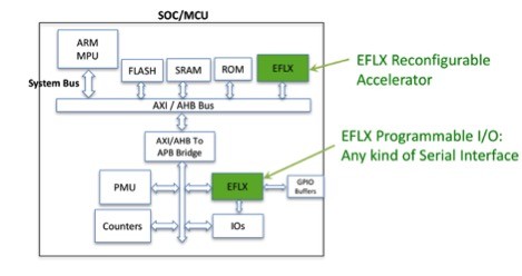
Figure 1. Flex Logix’ EFLX eFPGA IP can be implemented as a reconfigurable hardware acceleration block or reprogrammable I/O block in MCU and SoC designs.]
For chip designers working with the ARM architecture, for example, eFPGAs can be connected to an APB, AHB, or AXI processor buses to take advantage of these benefits. However, given the numerous combinations (master/slave x AXI/AHB/APB x external interface logic or implemented with the eFPGA), these designs should be carefully considered.
eFPGA I/O resources
For a better understanding of how an eFPGA can be designed into an ARM-based MCU or SoC using standard interfaces, we will use the Flex Logix EFLX-2.5K embedded FPGA IP core as an example.
The EFLX-2.5K eFPGA is a 1x1 array that consists of 2,520 six-input look-up tables (LUTs) with 632 inputs and 632 outputs. It operates at about 1 GHz in 16 nm processes and better than 500 MHz in 28 nm processes. Thus, even the smallest eFPGA has the I/O resources and speed sufficient to connect to the widest, fastest ARM buses.
(Note: Larger arrays of up to 7x7 are possible, with the number of I/O for each increasing array size calculated as N*632 inputs and N*632 outputs in an NxM array. The number of LUTs in increasing array sizes is similarly calculated as N*M*2520.)
eFPGA as an APB slave
An eFPGA configured as an APB slave will typically be implemented as a reconfigurable I/O function. For example, one of many kinds of serial interfaces can include UART, I2C, and SPI.
In this configuration, multiple blocks connect to the APB bus, which operates on one block at a time (Figure 2). Each block has memory mapped address space (such as 8 bits for 128 registers), while data on the bus can be 8, 16, or 32 bits. An 8-bit address space and 32-bit data requires 45 inputs and 33 outputs, while a 16-bit bus uses 16 fewer inputs and 16 fewer outputs.
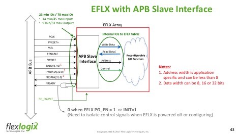
Figure 2. An eFPGA configured as an APB slave is typically implemented as a configurable I/O function that contains multiple memory mapped blocks. The APB bus synchronously operates on each of these.
The APB slave interface is fast, simple, and can be implemented externally or in the logic of the eFPGA. For example, less than 10 LUTs are required for an EFLX eFPGA in this configuration. As shown in Figure 3, APB slave interface Verilog code and state diagrams are short and simple as well.

Figure 3. Verilog code and state diagrams are simple when for eFPGAs configured as an APB slave interface.
eFPGA as an AXI master
The AXI bus consists of three versions: AXI4, AXI4 Stream, and AXI4 Lite.
Figure 4 shows an AXI4 master with a wrapper implemented externally to the eFPGA. The function of the AXI master wrapper is to handle all of the bus protocols, manage data flow control, and isolate the EFLX FPGA from the AXI bus during configuration.
Here, the EFLX Reconfigurable Accelerator acts as a bus master so that the CPU is not required to transfer data to and from memory. This offloads the CPU for other tasks that can run in parallel with the EFLX accelerator.
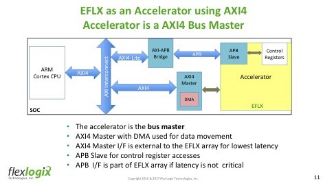
Figure 4. Configured as an AXI master, the EFLX Reconfigurable Accelerator can offload the CPU of bus management tasks.
The EFLX eFPGA is capable of supporting narrow or very wide (128 bytes) AXI data widths depending on the bandwidth required by the accelerator function. Control registers in the EFLX array and the APB slave logic are implemented in the EFLX array and controlled over the APB bus. The APB slave interface example shown in Figure 2 can implement the control register interface.
A high-level diagram of the AXI bus architecture is shown in Figure 5, illustrating a master-slave connection. When implementing an eFPGA as an AXI master, the eFPGA should always be flopped to simplify closing, timing, inputs, and outputs to/from. Data bus widths can be 1, 2, or 4 bytes and so on, up to 128 bytes.
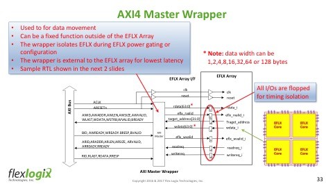
Figure 5. To simplify the master-slave connection in the AXI bus, it is recommended that the eFPGA be flopped.
Even for a complex bus master, Verilog code is relatively simple (Figure 6).

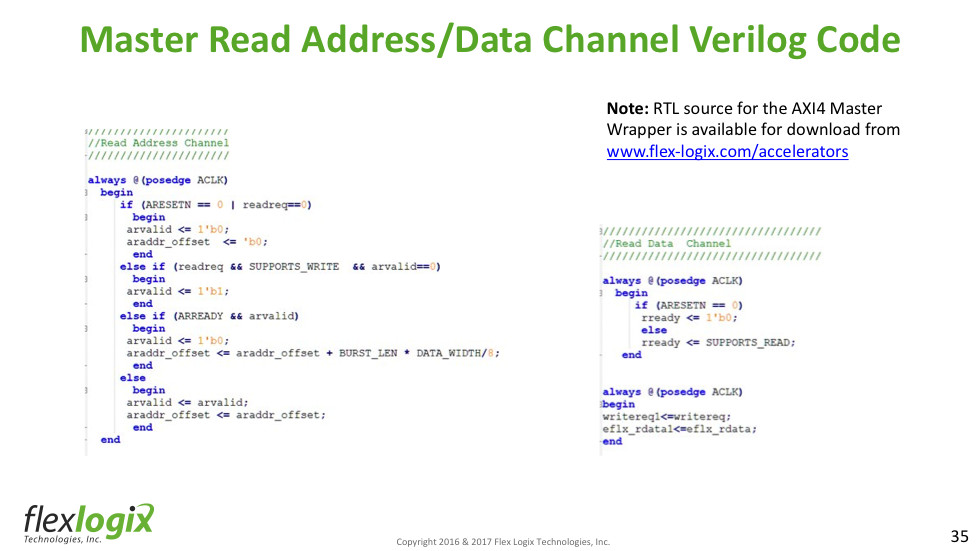
Figure 6. Verliog code remains relatively simple when using an eFPGA as an AXI bus master.
eFPGA over a separate slave interface
In addition to the bus connection for array operations as an accelerator or I/O processor, eFPGAs such as EFLX provide a separate slave interface for loading the configuration bits to be reconfigured as desired. An external AXI slave wrapper can also be used to interface with the configuration port.
Using EFLX, for example, configuration bits are typically stored in the same flash memory as the ARM processor code. After the processor boots it uses direct memory access (DMA) to access configuration bits through the configuration slave interface into the eFPGA.
Conclusion
With the growing need for flexibility and performance in modern processing solutions, eFPGAs can easily connect to any type and width of ARM bus using a small amount of high-speed logic. After years of complexity and cost challenges, reconfigurable accelerators and I/O processors based on eFPGA technology have become an easy-to-use resource for architects of any kind of ARM-based SoC or ASIC.
Tony Kozaczuk is director of solutions architecture at Flex Logix, Inc.
Flex Logix Technologies, Inc.


