
Understanding IoT requirements 101, part 2
April 12, 2017
Blog

In part one of Understanding IoT Requirements 101, we covered advanced process technology, low power design techniques, power considerations for multicore systems, inter-core communications,...
In part one of Understanding IoT Requirements 101, we covered advanced process technology, low power design techniques, power considerations for multicore systems, inter-core communications, serial memory interfaces, and system security. In part two, we will cover advanced BLE wireless links, smart touch interface, IoT sensors and interface, and analog front end.
Advanced wireless links
Connected IoT devices are still in their infancy. This means that as new applications arise, there will be demands on the system MCU to provide significant improvements in speed, power consumption, range and capacity. The potential business opportunities in this domain push the limits of engineering. The recent announcement by the Bluetooth Special Interest Group (SIG) regarding Bluetooth 5.0 is a prime example of how the electronics industry responds to IoT market demands.
As per the announcement, the new BLE standard will offer twice the speed, four times the range, and an 800 percent improvement in connectionless data broadcast. This will significantly improve how connected IoT devices interface with our day-to-day lives. As the MCU is the heart of IoT devices, it will have to keep pace with protocol advancements to support the benefits new standards have to offer. Here are some of the highlights of the upcoming BLE standard:
- Bluetooth 5.0 will be faster than Bluetooth 4.2 by a factor of two with a maximum theoretical throughput of 2 Mbps.
- The range will quadruple compared to earlier versions, extending up to 300+ meters.
- Protocol optimizations will enable better performance and power consumption.
- Protocol optimizations will showcase an 800 percent increase in data broadcasting capacities backed by industry-leading power performance.
- Enhanced encryption and authentication will allow only trusted users to track device locations and to confidently pair devices.
These features do not come for free, in terms of added processor capacity, memory, and power. For many applications, the underlying hardware will need to change to support these features. For this reason, MCU manufacturers must always keep these demands in mind when they design their next-generation MCU devices (Figure 1).
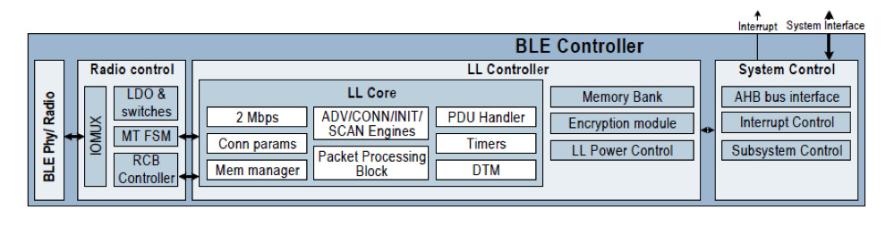
[Figure 1 | The Cypress PSoC 6 BLE MCU offers BLE 5.0 ready features to IoT designers.]
While increasing the load on the MCU, these features offer many benefits to end users.
Performance (range benefits)
BLE is becoming the wireless protocol of choice for designers developing IoT-based products. Improved range will ensure that any Bluetooth device (such as a speaker, smart lock, lightbulb, etc.) can be connected to flawlessly from anywhere in a house. This is a key step to enabling a true smart home. BLE 5.0 also has the potential to replace power-hungry Wi-Fi to control smart home devices. Improved range will also benefit devices such as smart watches to receive instant notifications from smartphones.
Power (speed benefits)
Higher transfer speeds improve responsiveness. For IoT devices that are typically not data-intensive, higher speed will manifest as lower power consumption and longer operating life. For example, twice the transfer speed reduces transmit / receive time by half. This enables power consumption to be reduce since the device can be put into a low-power mode sooner. In addition, higher transfer speed enables superior support for periodic device software updates. This will be a significant capability for IoT applications.
Connectionless services (broadcast capacity benefits)
The significant increase in the broadcast capacity will make information transmission richer and smarter. Connectionless services such as beacon will be able to transmit more information. For example, beacons will be able to transmit actual content instead of pointing at the content through a URL. This has a potential to redefine the way Bluetooth devices transmit information today by moving towards connectionless IoT instead of Bluetooth paired devices model. This has the potential to make BLE applications like asset-tracking and smart waste management smarter using mesh networks.
Smart touch interface
As discussed in part one, IoT devices span across consumer, industrial, and business applications. All these applications can benefit from a sleek user interface, with product-differentiating features such as a touch display, buttons/sliders and proximity sensing. For the best user experience, touch displays may also need to be able to support gesture recognition, water resistance, wrist detection, and gloved touch. Each of these features can be implemented using capacitive sensing technology in a manner that maintains low power consumption. Touch sensing can also help optimize power consumption, such as using proximity to sensing to detect when a user approaches the device to use it. Integrating capacitive sensing in the MCU eliminates the need for a separate dedicated sensing device. Integration also improves power efficiency, performance and cost (Figure 2).

[Figure 2 | PSoC 6 integrated with BLE connectivity and capacitive touch sensing]
Capacitive sensing is a key technology for enabling innovative new applications and product features.
Smart home switches
Enabling individuals to control home devices remotely offers many advantages. The same applies to home appliances. Two critical building blocks are required to enable smart home appliances. The first one is a wireless link, which connects the appliance to the cloud. The other element is an intelligent switch that can be controlled by multiple sources, such as the cloud, a remote control, smart phone, and/or physical user inputs.


[Figure 3 | Capacitive sensing-based smart home switches]
Smart switches with capacitive sensing can enable many advanced features:
- Smart Dimmer – Capacitive sensing sliders provide an intuitive, physical interface for dimmer capabilities. BLE enables the wireless interface for the dimmer so it can be placed anywhere in a room.
- Memory – The MCU can save the brightness setting selected in its internal Flash and restore settings between power interruptions or subsequent uses.
- Safety – Since the high voltage AC section of the smart switch is isolated to a relay, the physical user interface section only deals with low-power DC and thus assures user safety.
- Illumination – The MCU can provide LED-based illumination on the switch to enable users to locate the switch in dark conditions. This feature can be enabled using the capacitive-based proximity sensing.
- Gestures – With the ability to detect proximity and touch gestures, switches can be configured to perform specific tasks quickly and easily.
- Control – The development ecosystem supporting the IoT-based MCU with capacitive sensing simplifies managing the switch and enables multiple sources to control it.
Human body detection
As a technology, capacitive sensing can detect any conductive material in its range, including a human body (due to its mass). This enables a number of interesting features for IoT devices. For example, a wearable device needs to be able to detect whether the device is being worn or not for security and low-power considerations. The working principle is straightforward. The capacitive sensor detects the wrist whenever the users wears it and triggers the locking mechanism to protect vital data stored in it from viewing by other users. Similarly, when the device is not being worn, the device drops into low power operation mode. These actions help to extend battery life, a key consideration for any wearable application.


[Figure 4 | Wrist detection using capacitive sensing]
Capacitive touch sliders
Sliders are an important user input mechanism that helps people interact easily with IoT products. This feature is especially well suited for small form factor wearable devices, where having a large screen is not feasible. Very small touch screens makes it difficult to change device parameters or navigate through menus when the finger is blocking most of the screen. Capacitive-based sliders enable switching between various menus or screens with just a swipe (Figure 5). These same sliders can also act as capacitive touch buttons for entering data or selecting menus.

[Figure 5 | Capacitive touch sliders]
Capacitive touch displays
Touch displays provide a rich user interface for IoT devices with medium to large form factors, ranging from microwave oven to hand-held medical equipment, from smart watches to industrial controllers, etc. Typically, touch displays are implemented with capacitive sensing technology using a transparent Indium tin oxide (ITO) material over the display. Depending upon the application, the capacitive touch technology needs to be able to work reliably in wet operating conditions.

[Figure 6 | Capacitive touch displays]
Sleek user interface through gestures
Special gestures play a key role in enhancing the user experience. Gestures also help IoT manufacturers to differentiate their products in the marketplace. For example, a wireless Bluetooth speaker can be accessed directly using various hand gestures to adjust the volume, change the track, etc. Gestures tend to be one of the most intuitive forms of user interface. Smart gestures include swiping to either direction, left or right, single tap, double tap, long press, and so on. Gesture capabilities not only simplify the UI but also enable lower operating power since the device can be “woken up” by using a specific user gesture.

[Figure 7 | Capacitive touch and proximity gestures]
IoT sensors and interface
IoT applications are typically a combination of sensors, secure CPU, and a wireless link. Sensors are key to all IoT applications. Humans interact with their environment using their senses. Sensors can enrich human interaction with their surroundings.
![]()
[Figure 8 | PSoC 6 with integrated BLE connectivity and capacitive touch blocks]
All IoT applications use one or more sensors. These sensors are fundamentally either analog or digital in nature. Analog sensors output a continuous analog signal such as current or voltage. The magnitude of this signal correlates to sensor measurement. There are many types of analog sensors available in the market, including ambient-light sensors, temperature sensors, sound sensors, UV sensors, and so on.
Digital sensors, in contrast, convert and transmit data digitally. Because the signal measured is directly converted from analog to digital within the sensor, digital sensors are replacing analog sensors in many applications. Digital data is transmitted from the sensor through a cable or other transmission media with no transmission loss. Examples of common digital sensors are digital accelerometer sensors, digital pressure sensors, magnetometer, GPS, and so on.
Sensors, whether they are analog or digital, need an interface circuit to pass data to the IoT MCU. In the case of analog sensors, a signal-conditioning circuit is required to process/enhance the sensor output. These circuits are commonly referred as Analog Front-End (AFEs). AFEs consist of a biasing circuit, amplifier, comparators, digital to analog convertor (DAC), analog multiplexers, voltage references, a filter network for noise suppression and error suppression techniques like offset removal, and an analog to digital converter (ADC) to digitize the sensor data. In contrast, digital sensors need only a digital communication channel such as UART, I2C, or SPI to transfer sensor information to the MCU.
To connect a sensor to a traditional microcontroller requires the interface circuit to be built outside the chip, although some devices may have a fixed-function ADC integrated into the MCU. For IoT applications, a highly integrated MCU with a comprehensive set of analog and digital components is ideal.

[Figure 9 | PSoC 6 BLE AFE & DFE]
Analog front-end example for IoT applications
Consider a heart rate monitor (HRM) to understand the requirements of an AFE in IoT applications. A HRM requires an analog signal conditioning circuits to work reliably. There are various methods by which heart rate can be measured. The most popular methods are:
- Photoplethysmography (PPG)
- Electrocardiography (ECG)
- Phonocardiography (PCG)
Photoplethysmography (PPG)
PPG is an optical method to measure the cardiovascular pulse waves. The periodic pulsations of arterial blood volume cause pulse waves. The measuring method involves a light source and a photo-diode (receiver). In this method, the change in volume caused by the pressure pulse is detected by illuminating the skin with the light from an infrared LED and then measuring the amount of light either transmitted or reflected to a photodiode (Figure 10).

[Figure 10 | PSoC 6 BLE AFE circuit for the PPG method]
Electrocardiography (ECG)
As the heart undergoes de-polarization and re-polarization, electrical currents are generated that spread throughout the body. These electrical impulses can be detected by placing electrodes at specific points on the human body. An electrocardiogram (ECG) captures this varying electrical impulse to track the overall rhythm of the heart. These electrical signals, ranging from 0.1mV to 1.5mV, are due to cardiac muscle activation and are sensed between spaced points on the body. The potential difference between two spaced inputs points are amplified by op amps. The signal is than sampled by an ADC. ADC samples can be integrated and used to drive a compensating current into the amplifier’s feedback loop. The analog portions of this circuit can be shut down between samples in battery-powered units to save the power (Figure 11).

[Figure 11 | PSoC 6 BLE AFE circuit for the ECG method]
Phonocardiography (PCG)
The opening and closing of valves in the heart produces sounds during contraction and dilation that are normally audible through a stethoscope. The microphone is used to pick the heart beats and the resultant signal is used to measure the heart rate. These sounds are rhythmic to heart beat. This acoustic property is used in phonocardiographs to determine the heart rate. The electrical signals from the microphone are amplified and can be passed through a noise filter to remove external noises. Various sounds can be filtered from the ADC data using digital filters in order to calculate the heart rate (Figure 12).

[Figure 12 | PSoC 6 BLE AFE circuit for the PCG method]
Developers have a great many options when designing IoT devices. By understanding the various capabilities available in IoT-based MCUs, developers choose integrated processors that simplify design, improving performance, provide superior power efficiency, and lower overall system cost. In addition, developers can implement innovative features that improve ease of use and differentiate their products from others on the market.


