
Signal processing and the evolution of NAND flash memory
December 01, 2010
Signal processing can help bridge the gap between application needs and the inherent limitations of NAND flash.
Fueled by rapidly accelerating demand for performance-intensive computing devices, the NAND flash memory market is one of the largest and fastest-growing segments of the semiconductor industry, with annual sales of nearly $20 billion. During the past decade, the cost per bit of NAND flash has declined by a factor of 1,000, or a factor of 2 every 12 months, far exceeding Moore’s Law expectations. This rapid price decline has been driven by aggressive process geometry scale-down and by an increase in the number of bits stored in each memory cell from one to two and three bits per cell.
As a consequence, the endurance of flash memory – defined as the number of Program and Erase (P/E) cycles that each memory cell can tolerate throughout its lifetime – is severely degraded due to process and array impairments, resulting in a nonlinear increase in the number of errors in flash memory. Single-Level Cell (SLC) NAND, which was the mainstream NAND flash technology a few years ago, achieved 100,000 P/E cycles at 50 nm process node. Today’s mainstream Multi-Level Cell (MLC) two bits per cell NAND at 20 nm process node achieves only up to 3,000 P/E cycles, and three bits per cell NAND at the same process node achieves as low as a few hundred P/E cycles. Future process nodes are bound to yield even lower endurance.
Meanwhile, the migration of NAND flash from removable media storage to today’s memory- and performance-intensive mobile computing devices such as smartphones, tablets, and notebooks is driving up NAND flash endurance requirements. While USB flash drives and microSD cards, which comprised the core NAND market segments until recently, need only a few hundred P/E cycles, the NAND flash embedded in smartphones typically requires at least 3,000 P/E cycles. Enterprise-grade Solid-State Drives (SSDs) require as much as 50,000 P/E cycles.
Getting past errors
The most common approach to combating NAND flash endurance limitations is the use of Error Correction Code (ECC). ECC utilizes data checking and correction bits, also referred to as parity bits, which are stored on the NAND in addition to the application content, also referred to as data bits. For ECC to correct more bits, more parity bits must be stored, resulting in additional cost. An ECC scheme is usually characterized by the code rate, which is defined as the ratio between the number of data bits to the total number of stored bits (data + parity). Higher code rate is more cost-effective, but typically yields weaker correction capability and is therefore more sensitive to errors.
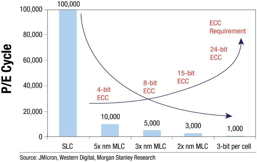
The most commonly used ECCs for flash memory are Bose-Chaudhuri-Hocquenghem (BCH) codes. Over the years, the correction capability of BCH codes for NAND flash memory has increased from correction of 4 bits in a sector of 512 bytes using code rate larger than 98 percent to correction of 24 bits in a double sector of 1,024 bytes using code rate of 96 percent. However, as illustrated in Figure 1, this by itself is not sufficient to maintain the endurance of the memory cell.
|
|
More advanced ECC schemes are capable of correcting more bits for a given code rate, such as Low-Density Parity-Check (LDPC) codes or turbo-codes. These codes use modern iterative decoders that enable fast and efficient error correction. Furthermore, unlike BCH, which uses hard decoding, these codes enable soft decoding, where in addition to each bit value, the decoder can also estimate the bit’s reliability. Soft decoding can yield significant correction capability gains over hard decoding, because the decoder knows which bits are more likely to be flipped and can use this information in its correction algorithms.
However, even the most modern and efficient ECC schemes are not effective when the number of errors is too large. For example, if a sector of 512 bytes has hundreds of bit errors, Claude Shannon’s information theory bounds show that no ECC can correct these errors with a reasonable and cost-effective code rate. Of course, if a very large number of parity bits is added, the errors can be corrected, but the cost impact is practically unacceptable.
Physical impairments of NAND flash memory
NAND flash memory is an array of cells. Each cell contains electrical charge, the amount of which indicates the information stored in the cell. The first NAND flash had two levels of charge and therefore stored one bit of information in each cell.
Today, most NAND flash has four or even eight levels and therefore stores two or three information bits per cell, respectively. The charge-storing elements (floating gates) of the cells are surrounded by isolating material so that their charge can be maintained for years without supplying power to the memory.
NAND flash suffers from a variety of impairments. A key impairment is leakage, which is a slow change of the cell’s charge due to electrons leaking through its isolation material over time. Another key type of impairment is a disturb, which is a change in the cell’s charge due to the potential difference applied to it while reading or programming the cell or its neighboring cells.
Because of the cells’ electrical isolation, a relatively high voltage must be applied to change the charge in the cell during P/E operations. This high voltage, which can reach dozens of volts, damages the cells, changes their characteristics, and magnifies their leakage and disturb characteristics. Damage to the cells is accumulated throughout P/E operations, degrading NAND endurance.
As the size of the cell reduces due to process geometry scale-down, the amount of electrons in the cell declines. Thus, in the latest flash process nodes, the difference between the charge levels in the cell amounts to less than 100 electrons. This magnifies the problems of leakage and disturbs, as even a few dozen electrons can change the logical level of the cell. The more condensed cell array also magnifies the floating gate coupling due to electric field coupling between adjacent cells.
The role of signal processing
Signal processing methods and algorithms have recently been applied to NAND flash to combat endurance limitations. These algorithms are used to compensate for the physical limitations of NAND flash, exploiting their unique nature and structure. For example, the floating gate coupling distortion in a cell can be measured and compensated for via signal processing algorithms.
Compared to traditional approaches, the use of signal processing algorithms in combination with soft ECCs requires more information transfer between controller and NAND array. Careful algorithm and system designs are required to avoid performance degradation due to this additional information transfer.
Anobit’s Memory Signal Processing (MSP) technology, which is being used today by leading manufacturers of smartphones, tablets, and personal media players, employs this new approach within the NAND controller. Figure 2 highlights the major components of an MSP-powered controller. The unique element is the signal processor, which comprises hardware accelerators designed to combat NAND flash process and array impairments such as floating gate coupling distortion, read and program disturbs, and data retention and endurance impairments. The signal processing engine is closely coupled to an advanced ECC engine, where the information flow between the two is a key factor for the solution’s impairment-combating ability. The signal processing engine is managed by a microcontroller, giving the solution enough flexibility to apply to a variety of NAND processes.
|
|

NAND flash memory is crucial to the continued growth of the consumer electronics market and the continued evolution of memory- and performance-intensive computing devices. Signal processing is emerging as a key technology to bridge the gap between application needs and the inherent limitations of NAND flash, preventing NAND’s physical impairments from compromising the market potential for next-generation NAND chips and the devices they power.
Anobit
+972-9-954-9560


