
Composite Amplifiers: High Output Drive Capability with Precision
September 06, 2019
Blog

A composite amplifier is an arrangement of two individual amplifiers configured in such a way as to realize the benefits of each individual amplifier while diminishing the drawbacks of each amplifier.
Introduction
It is normal, and almost expected, to be faced with applications for which a solution does not appear to exist. To meet their requirements would require us to think of a solution that is beyond the performance of current products that the market offers. For example, an application may require an amplifier that is high speed and high voltage with high output drive capability, but may also demand excellent dc precision, low noise, low distortion, etc.
Amplifiers that meet the speed and output voltage/current requirements and amplifiers with outstanding dc precision are readily available in the market—many of them, in fact. However, all the requirements may not exist in a single amplifier. When faced with this problem, some would think it is impossible for us to meet the demands of such applications, and that we must settle for a mediocre solution and go with either a precision amplifier or a high speed amplifier, perhaps sacrificing some of the requirements.
Fortunately, this is not entirely true. There is a solution for this in the form of a composite amplifier, and this article will show how it is possible.
The Composite Amplifier
A composite amplifier is an arrangement of two individual amplifiers configured in such a way as to realize the benefits of each individual amplifier while diminishing the drawbacks of each amplifier.
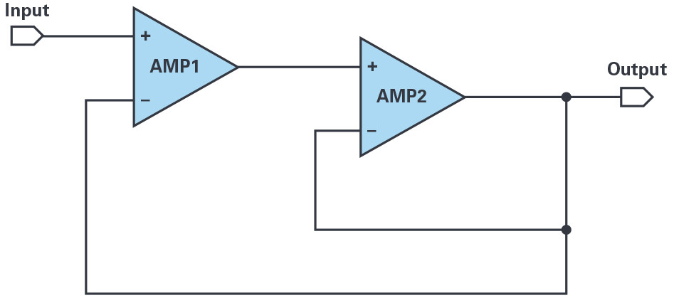
Referring to Figure 1, AMP1 should have excellent dc precision as well as the noise and distortion performance required by the application. AMP2 should provide the output drive requirements. In this arrangement, the amplifier (AMP2) with required output specifications is placed inside the feedback loop of an amplifier (AMP1) with the required input specifications. Some of the techniques and benefits of this arrangement will be discussed.
Setting the Gain
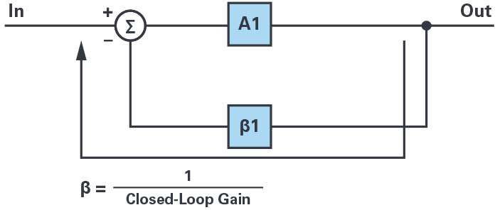
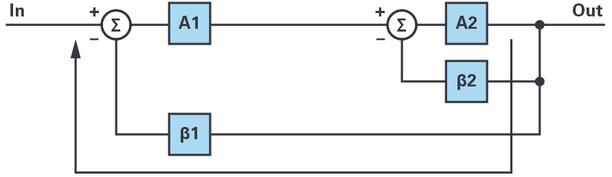
When initially encountering a composite amplifier, the first question that may arise is how to set the gain. To address this, it is helpful to view the composite amplifier as a single noninverting op amp contained within the large triangle, as in Figure 2. If we imagine the triangle is blacked out so that we couldn’t see what’s inside, then the gain of the noninverting op amp is 1 + R1/R2. Revealing the composite configuration inside the triangle doesn’t change anything—the gain of the whole thing is still controlled by the ratio of R1 and R2.
In this configuration it is tempting to think that changing the gain of AMP2 by means of R3 and R4 will affect the output level of AMP2, indicating a change in composite gain, but this is not the case. Increasing the gain around AMP2 via R3 and R4 will simply decrease the effective gain, and output level, of AMP1 such that the output of the composite (AMP2 output) remains unchanged. Alternatively, decreasing the gain around AMP2 will serve to increase the effective gain of AMP1. So, in general, the gain of the composite amplifier is only dependent on R1 and R2.

This article will discuss the major benefits and design considerations when implementing a composite amplifier configuration. The effects on bandwidth, dc precision, noise, and distortion will be highlighted.
Bandwidth Extension
One of the major benefits of implementing a composite amplifier is the extended bandwidth as compared to a single amplifier configured with the same gain.
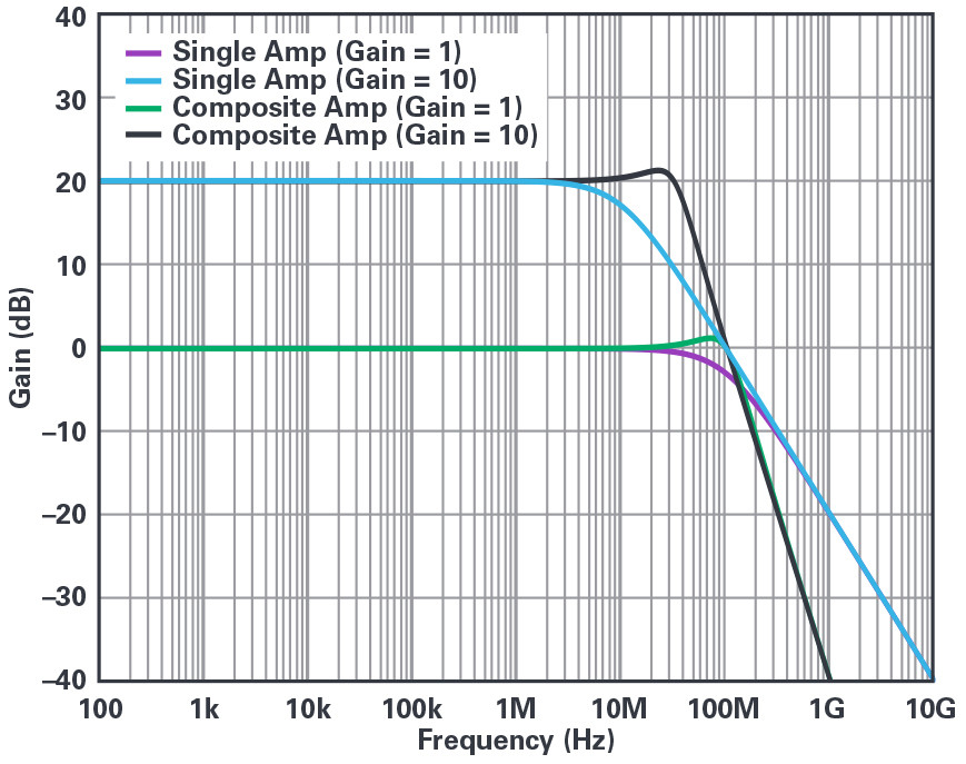
Referring to Figure 3 and Figure 4, let’s say we have two separate amplifiers each having a gain-bandwidth product (GBWP) of 100 MHz. Putting them together in a composite configuration will increase the effective GBWP of the combination. At unity gain, the composite amplifier offers a ~27 percent higher –3 dB bandwidth, albeit with a small amount of peaking. However, at higher gains this benefit becomes much more noticeable.
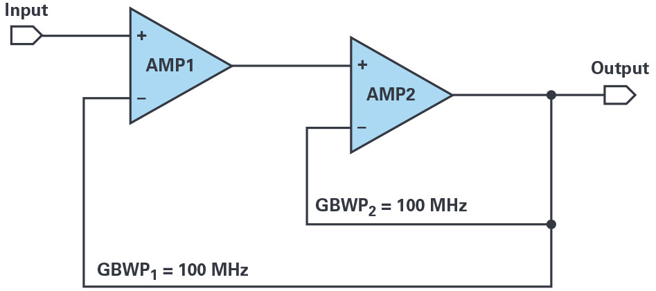
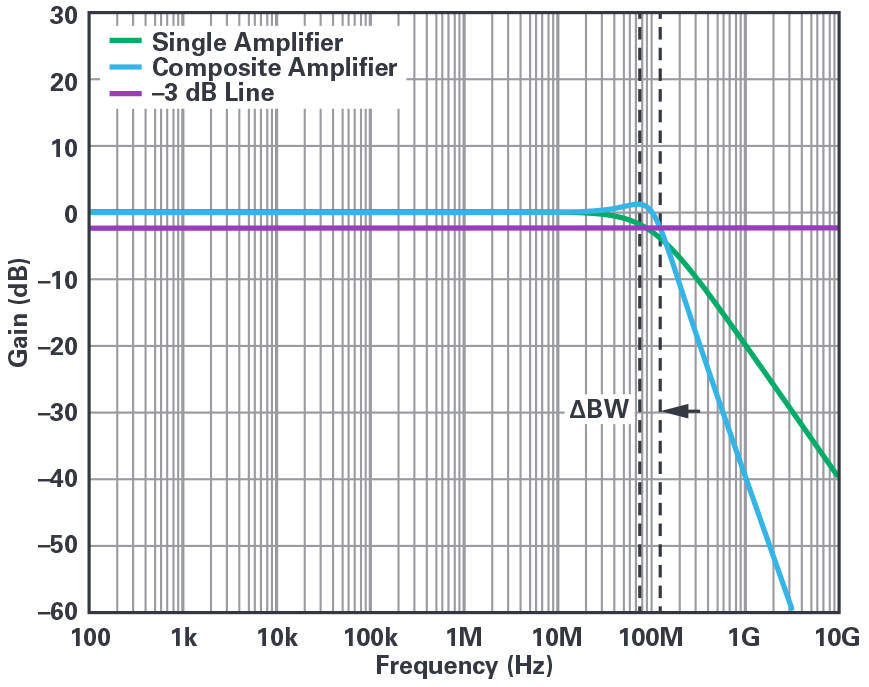
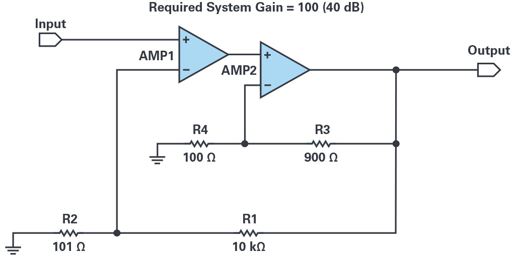
Figure 5 shows the composite amplifier in a gain of 10. Note the composite gain is set to 10 via R1 and R2. The gain around AMP2 is set to approximately 3.16, forcing the effective gain of AMP1 to be the same. Splitting the gain equally between the two amplifiers yields the greatest possible bandwidth.
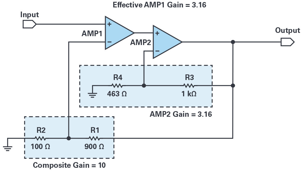
Figure 6 shows the frequency response for a single amplifier at a gain of 10 compared to a composite amplifier configured with the same gain. In this case, the composite offers a ~300 percent increase in –3 dB bandwidth. How is this possible?
For a specific example, refer to Figure 7 and Figure 8. We require a system gain of 40 dB and will use two identical amplifiers, each with an open-loop gain of 80 dB and a GBWP of 100 MHz.
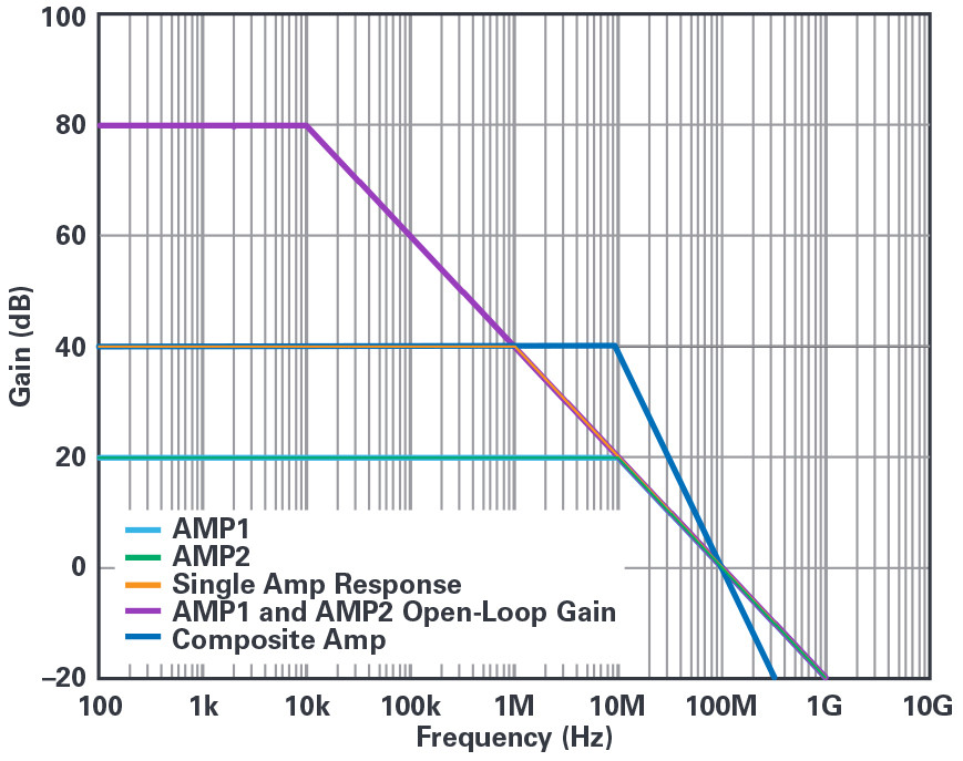
To realize the highest possible bandwidth for the combination, we will split the required system gain equally between the two amplifiers, giving each of them a gain of 20 dB. So, setting the closed-loop gain of AMP2 to 20 dB forces the effective closed-loop gain of AMP1 to 20 dB as well. With this gain configuration, both amplifiers operate lower on the open-loop curve than either of them would at a gain of 40 dB. As a result, the composite will have higher bandwidth at the gain of 40 dB as compared to the single amplifier solution of the same gain.
Although this may sound relatively simple and easy to implement, proper care should be taken in designing the composite amplifier to have the highest possible bandwidth without sacrificing the stability of the combination. In real-world applications where amplifiers are nonideal, and probably nonidentical, a proper gain arrangement must be ensured to maintain stability. Also, note that the composite gain will roll off at –40 dB/decade, so one must be careful when distributing the gain between the two stages.
In some cases, splitting the gain equally may not be possible. To that point, equal distribution of the gain between the two amplifiers requires that the GBWP of AMP2 must always be greater than or equal to GBWP of AMP1, otherwise peaking—and possibly instability—will result. In a case where AMP1 GBWP must be greater than AMP2 GBWP, the instability can typically be corrected by redistribution of the gain between the two amplifiers. In this case, reducing the gain of AMP2 causes an increase in the effective gain of AMP1. The result is that AMP1 closed-loop BW is decreased as it operates higher on the open-loop curve and AMP2 closed-loop bandwidth is increased as it operates lower on the open-loop curve. If this slowing down of AMP1 and speeding up of AMP2 is adequately applied, the stability of the composite combination is restored.
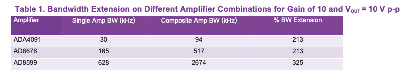
For this article, the AD8397 was picked as the output stage (AMP2), interfaced with various precision amplifiers for AMP1 to demonstrate the benefits of a composite amplifier. The AD8397 is a high output current amplifier capable of delivering 310 mA.
Preserved DC Precision
In a typical operational amplifier circuit, a portion of the output is fed back to the inverting input. Errors that are present on the output, which were generated in the loop, are multiplied by the feedback factor (β) and subtracted out. This helps maintain the fidelity of the output with respect to the input multiplied by the closed-loop gain (A).
For the composite amplifier, amplifier A2 has its own feedback loop, but A2 and its feedback loop are all inside the larger feedback loop of A1. The output now contains the larger errors due to A2, which are fed back to A1 and corrected. The larger correction signal results in the precision of A1 being preserved.
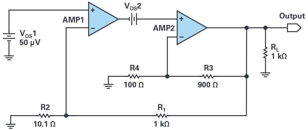
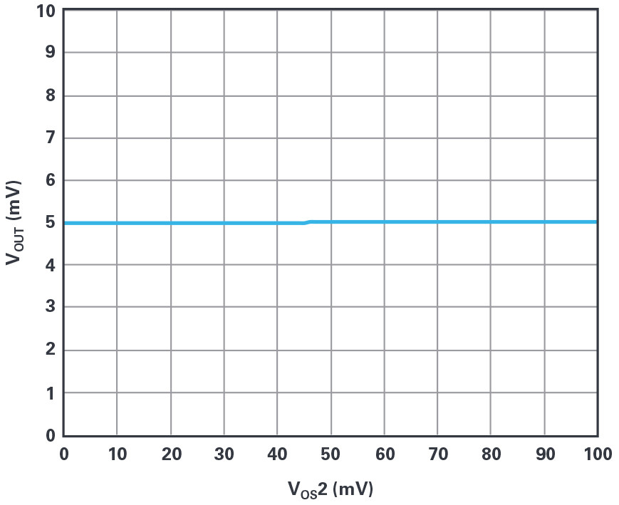
The effect of this composite feedback loop can be clearly seen in the circuit and results in Figure 11 and Figure 12. Figure 11 shows a composite amplifier comprised of two ideal op amps. The composite gain is 100 and the AMP2 gain is set to 5. VOS1 represents a 50 µV offset voltage for AMP1 while VOS2 represents a variable offset voltage for AMP2. Figure 12 shows that as VOS2 is swept from 0 mV to 100 mV, the output offset is not affected by the magnitude of error (offset) contributed by AMP2. Instead, the output offset is proportional only to the error of AMP1 (50 µV multiplied by the composite gain of 100) and remains at 5 mV regardless of the value of VOS2. Without the composite loop, we would expect the output error to increase as high as 500 mV.
Noise and Distortion
The output noise and harmonic distortion of the composite amplifier are corrected in a similar fashion as the dc errors, but, in the case of ac parameters, the bandwidth of the two stages also comes into play. We will look at an example using output noise to illustrate this with the understanding that distortion cancellation occurs in much the same manner.
Referring to the example circuit in Figure 13, for as long as the first stage (AMP1) has enough bandwidth, it will correct for the larger noise of the second stage (AMP2). As AMP1 begins to run out of bandwidth, the noise from AMP2 will begin to dominate. However, if AMP1 has too much bandwidth, and peaking is present in the frequency response, a noise peak will be induced at the same frequency.
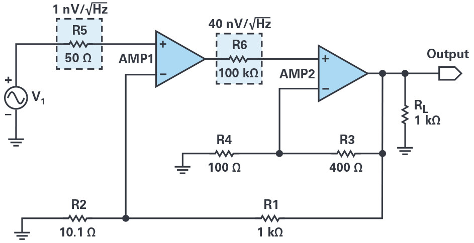
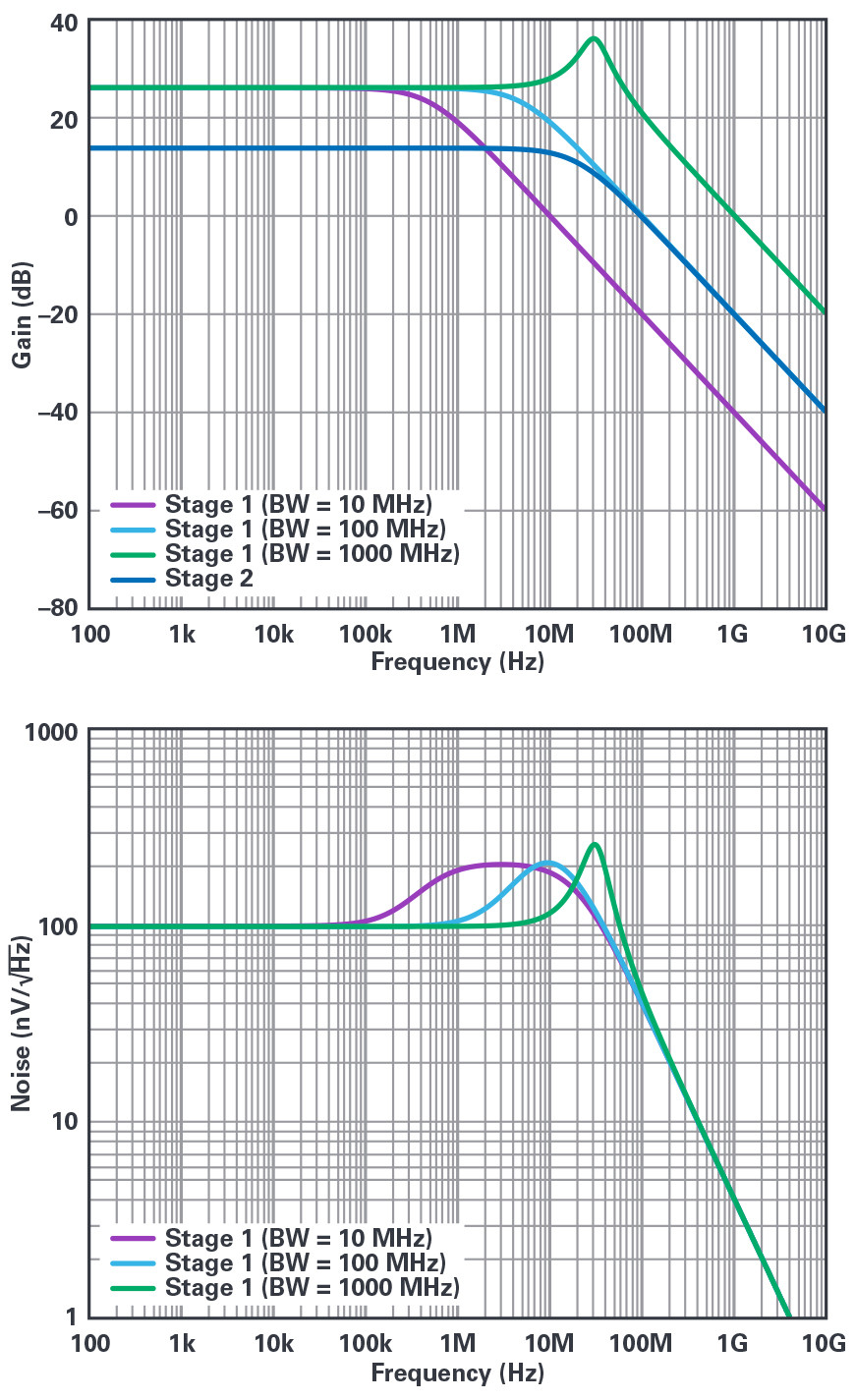
For this example, resistors R5 and R6 in Figure 13 represent the inherent noise sources for AMP1 and AMP2 respectively. The top plot of Figure 14 shows the frequency response for various AMP1 bandwidths as well as that of AMP2 for a single fixed bandwidth. Recall from the section on gain splitting that a composite gain of 100 (40 dB) and AMP2 gain of 5 (14 dB) will force an effective AMP1 gain of 20 (26 dB) as can be seen here.
The bottom plot shows the wideband output noise density for each case. At low frequencies, the output noise density is dominated by AMP1 (1 nV/√Hz times the composite gain of 100 equals 100 nV/√Hz). This will continue for as long as AMP1 has enough bandwidth to compensate for AMP2.
For the cases where AMP1 has less bandwidth than AMP2, the noise density will begin to be dominated by AMP2 as AMP1 bandwidth begins to roll off. This can be seen in two of the traces of Figure 14 as the noise climbs to 200 nV/√Hz (40 nV/√Hz times the AMP2 gain of 5). Lastly, in the case where AMP1 has much greater bandwidth than AMP2, resulting in a peaking in the frequency response, the composite amplifier will exhibit a noise peak at the same frequency, also shown in Figure 14. Since the frequency response peaking results in excessive gain, the amplitude of the noise peak will also be higher.
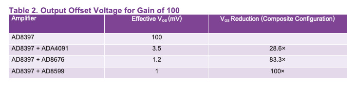
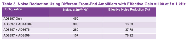
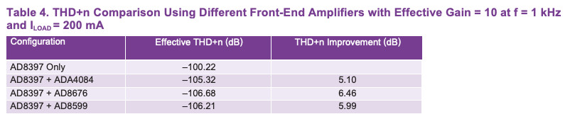
Table 3 and Table 4 shows the effective noise reduction and the THD+n improvement when using various precision amplifiers as the first stage in a composite amplifier with the AD8397.
System-Level Application
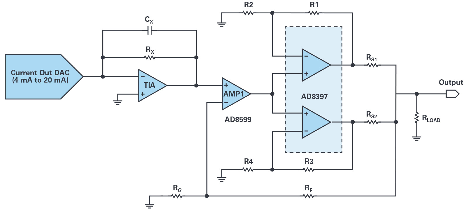
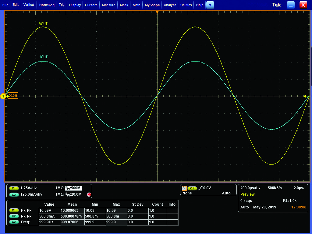
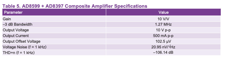
In this example, the goal for a DAC output buffer application is to provide an output of 10 V p-p into a low impedance probe with a current of 500 mA p-p, low noise and distortion, excellent dc precision, and as high of a bandwidth as possible. The output of a 4 mA to 20 mA current-out DAC is to be converted to a voltage by the TIA, then to the input of the composite amplifier for more amplification. With AD8397s on the output, the output requirements are attainable. AD8397 is a rail-to-rail, high output current amplifier capable of delivering the needed output current.
AMP1 could be any precision amplifier that has the desired dc precision needed for the configuration requirement. In this application, various front-end precision amplifiers could be used with AD8397 (and other high output current amplifiers) to attain both the excellent dc requirements and the high output capability drive needed for the application.
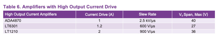
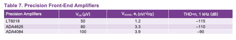
This configuration is not limited to AD8397 and AD8599, but is possible with other combinations of amplifiers to cater this output drive specification that requires excellent dc precision. The amplifiers in Table 6 and Table 7 are also suited for this application.
Conclusion
With the composite amplifier, the marriage of two amplifiers realizes the best specifications that each one offers while compensating for their limitations. Amplifiers with high output drive capability combined with precision front-end amplifiers could provide solutions to applications with challenging requirements. When designing, always consider stability, noise peaking, bandwidth, and slew rate for optimum performance. There are plenty of possible options to cater a wide range of applications. With the proper implementation and combination, striking the right balance for the application is highly achievable.
Acknowledgements
I would like to thank Zoltan Frasch and Bruce Petipas for their technical contributions to this article.
About the Author
Jino Loquinario joined ADI in 2014 and works as a product applications engineer for the Linear Products and Solutions Group. He graduated from Technological University of the Philippines–Visayas with a bachelor’s degree in electronics engineering.
To learn more about Power Electronics, check out:
KDPOF Offers Optical Connectivity
Maxim Class D Audio Amp Pumps Up the Volume
Composite Amplifiers: High Output Drive Capability with Precision


