
Architecture Exploration of AI/ML Applications and Processors
August 10, 2020
Story
Architecture exploration of AI applications is complex and involves multiple studies. To start with, we can target a single problem such as memory access or can look at the full processor or system.
Industry Background
Artificial Intelligence (AI) applications take into consideration the compute, storage, memory, pipeline, communication interface, software, and control. Further, AI application processing can be distributed across multi-core within processors, multiple processor boards on a PCIe backbone, computers distributed across an ethernet network, high-performance computer, or system across a data center. In addition, AI processors also have a massive memory size requirement, access time limitation, distribution across analog and digital, and hardware-software partition.
Problem
Architecture exploration of AI applications is complex and involves multiple studies. To start with, we can target a single problem such as memory access or can look at the full processor or system. Most designs start with the memory access. There are so many options- SRAM vs DRAM, local vs distributed storage, in-memory compute, and caching the back-propagation coefficients vs discarding.
The second evaluation sector is the bus or network topology. The virtual prototype can have a Network-on-Chip, TileLink or AMBA AXI bus for the processor internals, PCIe or Ethernet to connect the multi-processor boards and chassis, and Wifi/5G/Internet routers to access the data center.
The third study using the virtual prototype is the compute. This can be modeled as processor cores, multi-processor, accelerators, FPGA, Multi-Accumulate, and analog processing. The last piece is the interface to sensors, networks, math operations, DMA, custom logic, arbiters, schedulers, and control functions.
Moreover, the architecture exploration of AI processor and systems is challenging as it applies data-intensive task graphs on the full power of hardware.
Model Construction
At Mirabilis, we use VisualSim for the architectural exploration of AI applications. Users of VisualSim assemble a virtual prototype very quickly in a graphical discrete-event simulation platform with a large library of AI hardware and software modeling components. The prototype can be used to conduct timing, throughput, power consumption, and quality of service trade-off. Over 20 templates of AI processor and embedded systems are provided to accelerate the development of new AI applications.
Reports generated for the trade-off in AI systems include response times, throughput, buffer occupancy, average power, energy consumption, and resource efficiency.
ADAS Model Construction
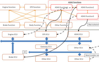
To begin with, let us consider the Autonomous Driving (ADAS) application, a form of AI deployment in Figure 1. The ADAS application co-exists with a number of applications on both the computer or Electronic Control Unit (ECU) and on the Network. There is also dependency on the sensors and actuators of the existing system for the ADAS task to operate correctly.

Figure 1. Logical to Physical Architecture of the AI Applications in an Automotive Design
Early architecture trade-off can test and evaluate the hypothesis to quickly identify bottlenecks, and optimize the specification to meet the timing, throughput, power, and functional requirements. In Figure 1, you will see that the Architecture model requires the hardware, network, application task, sensors, attenuators, and the traffic stimulus to gain visibility into the operation of the complete system. Figure 2 shows the implementation of this ADAS logical architecture mapped to the Physical Architecture.
A nice feature of the Architecture model is the ability to separate all parts of the design, such that the performance of individual operations can be studied. In Figure 2, you will notice the existing tasks are listed separately, the network with the ECUs, sensor generation, and the ADAS logical tasks organization. Each function in the ADAS task graph is mapped to an ECU.

Figure 2. System Model of Automotive System with ADAS Mapped to the ECU Network
ADAS Analysis
When the ADAS model in Figure 2 is simulated, you can get a variety of reports. In Figure 3, the latency to complete the ADAS tasks and the associated heat dissipated by the battery for this task are shown. Other plots of interest can be the measured power, network throughput, battery consumption, CPU utilization, and buffer occupancy.

Figure 3. Analysis reports from the ADAS Architecture Model
Processor Model Construction
Designers of AI processors and systems conduct experiments with application type, training vs inference, cost point, power consumption, and size limitations. For example designers can assign child networks to pipeline stages, trade-off deep neural networks (DNNs) vs conventional machine learning algorithms, measure algorithm performance on GPU, TPU, AI processors, FPGA and conventional processors, evaluate the benefits of melding compute and memory on a chip, compute the power impact of analog techniques that resemble human brain functions, and building SoCs with a partial set of functions targeted at a single application.
The schedule from PowerPoint to first prototype for the new AI processors is extremely short and the first production sample cannot have any bottlenecks or bugs. Hence modeling becomes mandatory.
Figure 4 shows the internal view of the Google Tensor Processor. The block diagram has been translated into an architecture model in Figure 5. The processor receives requests from a host computer via a PCIe interface. MM, TG2, TG3, and TG4 are different requests streams from independent hosts. The weights are stored in an off-chip DDR3 and called up into the Weight FIFO. The arriving requests are stored and updated in the Unified Local Buffer and sent to the Matrix Multiple Unit for processing. When the request has been processed through the AI pipeline, it is returned to the Unified Buffer to respond back to the Host.

Figure 4. TPU-1 from Google

Figure 5. Top view of a VisualSim Model of the AI hardware architecture
Processor Model Analysis
In Figure 6, you can view the latency and the Back-propagation weights management in the off-chip DDR3. The latency is from the time that the host sends requests to the receiving the response. You will see that TG3 and TG4 were able to maintain a low latency until 200 us and 350 us respectively. MM and TG2 started to buffer early in the simulation. As there is considerable buffering and the latency is increasing for this set of traffic profiles, the current TPU configuration is inadequate to handle the loads and the processing. The higher priority of TG3 and TG4 helped sustain operations for a longer period.

Figure 6. Statistics for the Architecture Exploration trade-off
Automotive Design Construction

Figure 7. Automotive Network with CAN Bus, Sensors and ECU
Today’s automotive design incorporates a number of safety and autonomous driving features that require a significant amount of machine learning and inference. The available time schedule will determine whether the processing is done at the ECU or sent to a Data Center. For example, a braking decision can be done locally while changing the air-conditioning temperature can be sent for remote processing. Both require some amount of artificial intelligence based on the input sensors and cameras.
Figure 7 is a network block diagram that incorporates the ECU, CAN-FD, Ethernet, and Gateway.

Figure 8. VisualSim model of an Autonomous Driving and E/E Architecture
Figure 8 captures a portion of Figure 7 that integrates the CAN-FD network with the high-performance Nvidia DrivePX that contains multiple ARM cores and a GPU. The Ethernet/TSN/AVB and Gateway have been removed from the model to simplify the view. In this model, the focus is on understanding the internal behavior of the SoC. The application is a MPEG video capture, processing, and rendering that is triggered by the camera sensors on the vehicle.
Automotive Design Analysis
Figure 9 shows the statistics for the AMBA bus and the DDR3 memory. You can see the distribution of the workload across multiple masters. The application pipeline can be evaluated for bottlenecks, identifying the highest cycle time tasks, memory usage profile, and the latency for each individual task.

Figure 9. Bus and memory activity report
The use cases and traffic patterns are applied to the architecture model assembled as a combination of hardware, RTOS, and networks. A periodic traffic profile is used to model the radars, lidars, and cameras while the use case can be autonomous driving, chatbot, search, learning, inference, large data manipulation, image recognition, and disease detection. The use case and traffic can be varied for the input rates, data sizes, processing time, priority, dependency, prerequisites, back-propagation loops, coefficients, task graph, and memory accesses. The use case is simulated on the system model by varying the attributes. This results in a variety of statistics and plots to be generated including cache hit-ratio, pipeline utilization, number of requests rejected, watts per instruction or task, throughput, buffer occupancy, and state diagram.

Figure 10. Measure the power consumption in real-time for an AI processor
Figure 10 shows the power consumption of both the system and silicon. In addition to the heat dissipated, battery charge consumption rate, and the battery lifecycle change, the model can capture the dynamic power change. The model plots the state activity of each device, the associated instant spikes, and average power of the system. Getting early feedback on the power consumption helps the thermal and mechanical teams to design the casing and the cooling methods. Most chassis’ have a maximum power constraint for each board. This early power information can be used to perform architecture trade-offs with performance, thus looking for ways to reduce power consumption.
Further Exploration Scenarios
The following are some additional examples highlighting the use AI architecture model and analysis.
1. Autonomous driving system with 360-degree laser scanner, stereo camera, fisheye camera, millimeter-wave radar, sonars, or lidars connected to 20 ECUs on multiple IEEE802.1Q networks connected via Gateways. The prototype is used to test feature packages for hardware configurations of the OEM to determine the hardware and network requirements. The response time for an active safety action is the primary criteria.
2. Artificial Intelligence Processor for learning and inference tasks is defined using a Network-on-Chip backbone that is built-up with 32 cores, 32 accelerators, 4 HBM2.0, 8 DDR5, multiple DMAs, and full cache coherency. This model is experimented with variations of RISC-V, ARM Z1, and a proprietary core. The goal achieved was 40Gbps on the links while maintaining a low Router frequency and retraining the network routing.
3. A 32-layer deep neural network needed to get the memory from 40GB to less than 7GB. The data throughput and the response times were not changed. The model is setup with the functional flow diagram of the behavior with the memory accesses for both the processing and the backpropagation. For different data sizes and task graph, the model determined the amount of discarding of the data and various off-chip DRAM sizing and SSD storage options. The task graph was varied with arbitrary number of graphs and several inputs and outputs.
4. General-purpose SoC using ARM processors and AXI bus for low-cost AI processing. The goal was to get the lowest power per watt which maximizes the memory bandwidth. The multiply-accumulate functions were off-loaded to vector instructions, encryption to an IP core, and the custom algorithms to accelerators. The model was constructed with the explicit purpose of evaluating different cache-memory hierarchy to increase the hit-ratio and bus topologies to reduce latency.
5. Analog-Digital AI processor requires a thorough analysis of the power consumption and an accurate analysis of the throughput achieved. In this model, the non-linear control was modeled in a discrete-event simulator as a series of linear functions to accelerate the simulation time. In this case, the functionality was tested to check the behavior and the measure the true power savings.
For more information, visit: https://www.mirabilisdesign.com


