
When Good Electrons Go Bad: How to Protect Your Analog Front End
April 17, 2019
Blog

The aim of this article is to help guide system designers in understanding different types of electrical overstress (EOS) and how it may affect their system.
The aim of this article is to help guide system designers in understanding different types of electrical overstress (EOS) and how it may affect their system. While this article targets specific types of electrical stress caused in systems, the information can still be applied to a variety of scenarios.
This topic is important because without proper protection, even the best circuits can degrade in performance or become destroyed by EOS.
What is EOS?
EOS is a general term that describes a system getting stressed by too many electrons trying to make their way into your circuit. It is important to remember that this is a function of power and time.
It may help to abstract a complex circuit as one simple component that dissipates power—say, a resistor. Put 1.1 V across a 1 Ω resistor rated at 1 W and the equation for power dissipated,
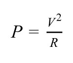
tells us 1.21 W is being dissipated. While the resistor is rated at 1 W, there is probably some margin built into it, so you may be able to get away with that for a while. Likely not forever, though.
What if you increased the voltage to 2 V? Smart money is on that resistor serving as a space heater for a very limited amount of time given that it is dissipating four times the previous example—remember:

What if you increased that voltage to 10 V, but only for 10 ms? That is where things get interesting—there is no way to really tell the effects on the part without understanding it and what it is designed to handle. Now we can take this knowledge to a whole system of components.
What is susceptible to EOS?
In general, everything that has electronics is susceptible to EOS. Particularly vulnerable parts are ones that interface with the outside world since they are likely to be the first to see electrostatic discharge (ESD), lightning strikes, and so on. Of interest to us are parts like USB ports, the analog front ends of oscilloscopes, and the charging port of the latest high performance IoT blenders.
How do we know what to protect against?
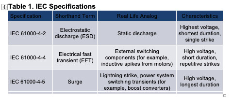
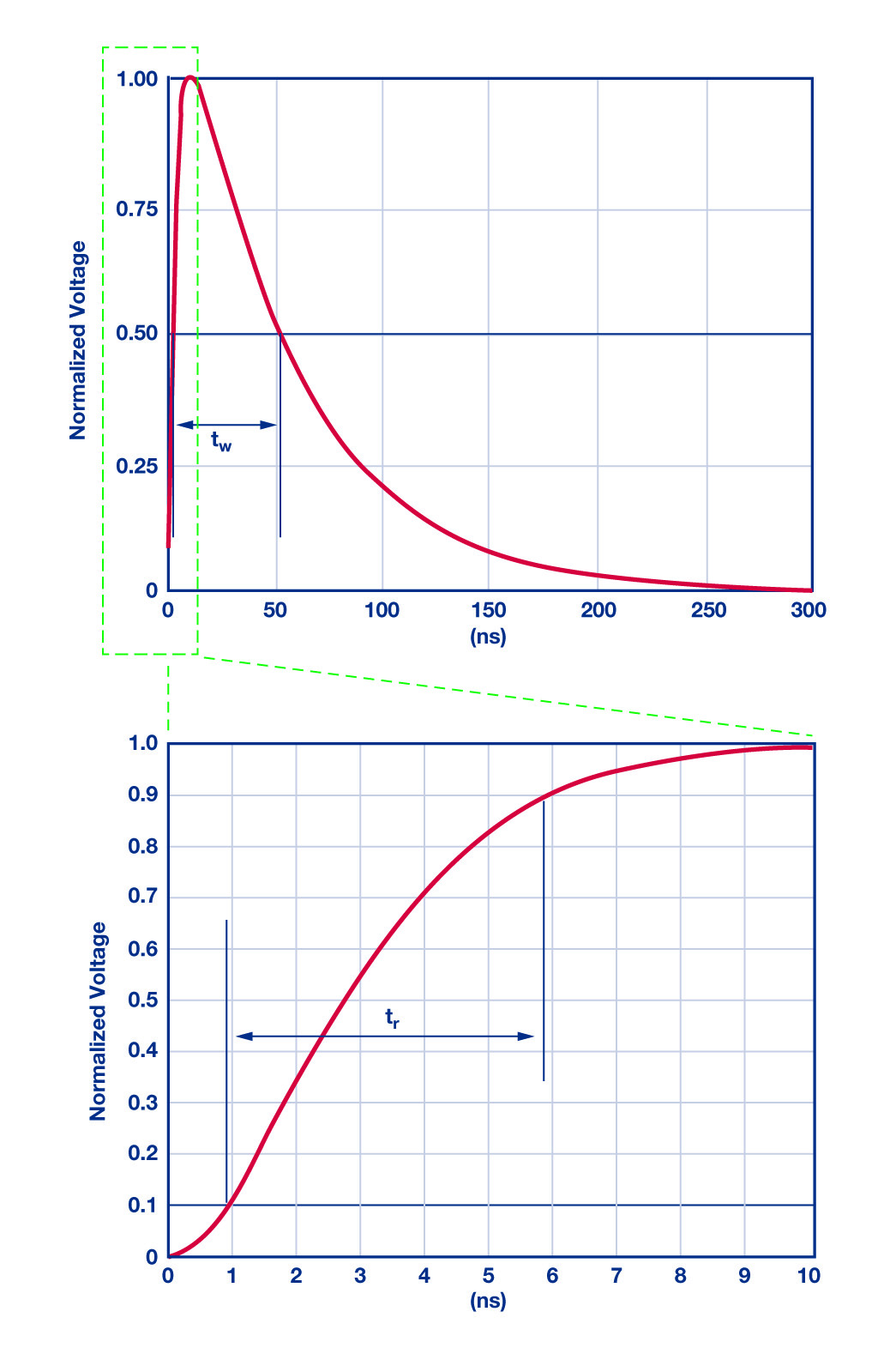
While we know that we want to protect a system against electrical overstress, that term is way too broad to be helpful when it comes to deciding how to protect our system. This is why the fine folks at the IEC (and many other organizations) have done the hard work of figuring out what types of EOS we are likely to encounter in real life. We will focus on IEC specifications since they cover broad market applications and the confusion around them justifies this publication. Table 1 shows three of the specifications that define just what type EOS conditions a system may encounter. While only ESD will be discussed in depth here, we should be familiar with electrical fast transients (EFT) and surge as well.
Haven’t the people who made the integrated circuits already protected the chips against ESD?
The unsatisfying answer to this is yes and no. Yes, these chips are designed to handle ESD in situations where they are being handled for manufacturing—not in situations where they are in systems and powered. This distinction is very important because when an amplifier has power supplied to it, it may behave very differently when exposed to static electricity than if it were not connected to anything. For example, an ESD strike on an unpowered part may be dissipated by the internal protection diodes. An ESD strike on a powered part, however, may cause internal structures to conduct more current than they are designed to handle. This may result in the part immolating itself depending on the part and the supply voltages.
This is an international emergency! How can I protect my favorite ICs from this looming threat?
As I hope you are realizing, there are so many elements to this challenge that a simple solution cannot be applied to all situations. The following is a list of factors that will determine whether a part survives an EOS event. It is split into two groups: factors we have no control over and factors we may have control over.
Things we have no control over:
- IEC waveform: ESD, EFT, and surge all have very different profiles, therefore they will exploit certain weaknesses of the devices they hit differently.
- Process technology of device being considered: Some process technologies are more vulnerable to latch-up than others. For example, CMOS processes are prone to latch-up but there are ways of mitigating that hazard through careful design and trench isolation used in many modern processes.
- Internal structures of device being considered: There are so many ways ICs are designed that a protection scheme that works for one may not work for another. For example, many devices have timing circuits that will turn on protection structures if a fast enough waveform is detected. That may mean that a device that survives an ESD strike may not survive if you add enough capacitance to the location of the strike. This response is counter-intuitive, but it is very important to realize: a common method of circuit protection—an RC filter—may make the problem worse.
Things you may have control over:
- PCB layout: The closer your parts are to the location of a strike, the more likely they are to see a higher energy waveform. This is because as the waveform of the strike is traveling down a path, the waveform is dissipating energy—in EMI radiating out from the path of the waveform, heat due to the resistance of the path, and parasitic capacitive and inductive coupling to nearby conductors.
- Protection circuitry: This is where we can have the most meaningful impact on the survivability of the device. The things above that we do not have control over will inform how we design a protection scheme.
You guys have those cool over voltage protection (OVP) and over the top (OTT) features. How about I use them to protect against high voltage transients?
No! Don’t do that. Not a good idea. The OVP and OTT features allow the inputs of a part to see voltages that are beyond the supply voltages with zero damage to the part. Relying on those features to protect against high voltage transients is like relying on rain boots to protect against a pressure washer. Rain boots are for puddles shallower than their height, just like OVP and OTT are for voltages lower than their rating. The voltage rating of OVP and OTT are on the order of tens of volts beyond a given supply rail. This will not help against 8,000 volts.
How do I know what protection circuitry will work?
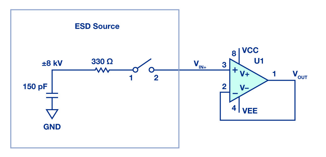
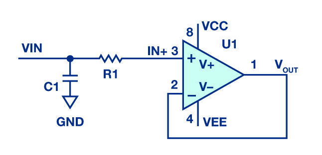
By using a combination of device knowledge, experience, and testing we can get a reasonable idea of what the optimal components to use in our system would be. Since there is a dizzying list of protection components that various manufacturers offer to keep things manageable, I will only discuss two circuit protection schemes that have proven effective in analog front-end protection. The following schemes assume an operational amplifier in buffer configuration. This is believed to be the most punishing test of protection because the noninverting input sees all the strike with no other areas for the energy to go (before protection is installed).
Considerations:
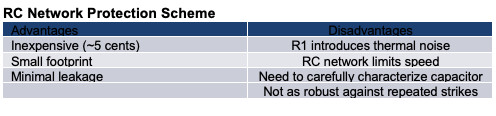
- R1 should be a pulse withstanding (thick film) resistor so that it will not break down so easily against high voltage transients.
- R1 voltage noise is proportional to the square root of the resistor value—an important consideration if the system needs to be low noise.
- C1 should be a ceramic capacitor with at least 0805 package size to mitigate surface arcing over the package.
- C1 should be at least X5R (ideally C0G/NP0) temperature coefficient to maintain predictable capacitance.
- C1 should be as low series inductance and resistance as possible so it can effectively absorb the strike.
- C1 should be as high a voltage rating as possible (minimum 100 V) for the given package size.
- C1 is before R1 in this case because it creates a capacitive divider with the 150 pF capacitor (from Figure 5) discharging the ESD waveform into our system, which shunts energy away before the amplifier sees it.
Note: While this method of front-end protection is not endorsed by capacitor manufacturers, it has been demonstrated to be effective over hundreds of tests on amplifiers. The ESD testing profile (explained below) has only been tested on a limited range of capacitor products, so if different ones are used, it is important to characterize how they handle strikes, such as by measuring capacitance and series resistance before and after ESD strikes. The device should maintain capacitance and always be open at dc frequencies after it is abused.
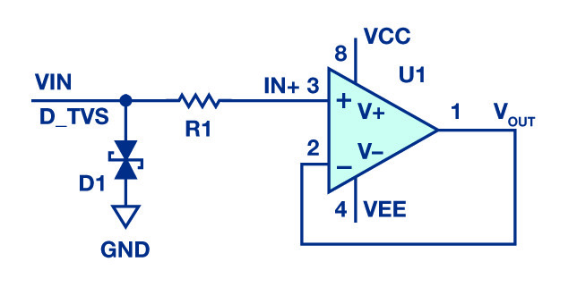
Considerations:
- Same as with an RC network: R1 should be pulse withstanding and noise may need to be considered.
- D1 should be specified for standards that need to be complied with. Some may only cover ESD, but others cover EFT and surge standards.
- D1 should be bidirectional so that it can handle both positive and negative strikes.
- The D1 reverse working voltage should be selected to be as high as possible while still passing necessary tests. Too low and it could leak current during normal system voltage levels. Too high and it may not react before the system is damaged.
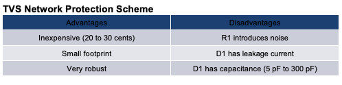
But I heard TVS diodes leak a lot and would kill my performance.
Common wisdom in analog electronics has dictated that TVS diodes are leaky and therefore cannot be used in precision analog front ends. This wisdom is not necessarily the case—many data sheets will show a leakage current of <100 µA, which is quite high for most analog folks. The issue with this number is that it is taken at maximum working voltage at maximum temperature (150°C). In this case, the diode will be extremely leaky. All diodes leak a lot more above 85°C. So long as one chooses a TVS diode with a higher reverse working voltage and doesn’t expect low leakage above 85°C, then one can expect much lower leakage currents.
You may be surprised with how little leakage is associated with a TVS if you select one properly. Figure 7 shows data taken measuring the leakage of 12 TVS diodes with the same part number:
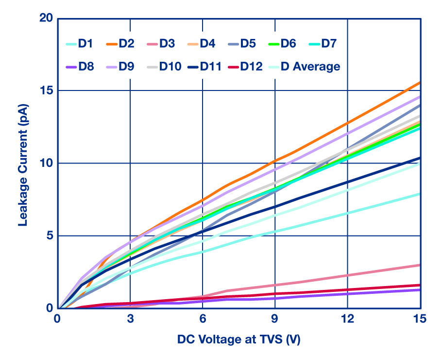
Out of 12 TVS diodes measured, the worst offender had 7 pA of leakage at a dc bias of 5 V. That is over 10 million times better than the data sheet worst-case scenario. Naturally, there is variation from batch to batch of TVS diodes in terms of leakage, but this should at least illustrate the order of magnitude of what to expect. If our system will not be seeing temperatures higher than 85°C, TVS diodes may be a good option. Just remember to characterize leakage if you choose other products than ones specifically tested here. What may be true for one part or manufacturer may not be true for another.
Testing Results:
A series of operational amplifiers were tested using the IEC ESD standards. Table 2 shows which protection schemes protect which components. Even though the ESD standard is three strikes at ±8 kV, all these schemes passed at 100 strikes at ±9 kV to ensure enough margin of protection.
IEC standards call for the ESD source ground to be connected to the amplifier’s ground via two 470 kΩ resistors in parallel with 30 pF of capacitance. This test setup was harsher because the ground of the ESD source was directly connected to ground of the amplifier. These results were also validated on the IEC ground coupling scheme just described for additional confidence. Keep in mind that since amplifiers have vastly different internal structures, what works for the devices on this list may
or may not work for others. It is recommended that if another device or other protection components are used, they be tested thoroughly.

Protection components used:
- Resistors: Panasonic 0805 ERJ-P6 series
- Capacitors: Yageo 0805 100 V C0G/NPO
- TVS diodes: Bourns CDSOD323-T36SC (bidirectional, 36 V, low leakage, rated for ESD, EFT, surge standards)
- ESD varistors: Bourns MLA series, 0603 26 V
Bonus component: ESD varistors
TVS diodes work great and can be struck an indefinite number of times. This feature is great for EFT and surge, but if all you need is ESD protection, look at ESD varistors—they are extremely high value resistors until they see a certain voltage, then they turn into low value resistors and shunt the energy through the varistor.
They are used in the same configuration as a TVS diode. They leak less and cost less than half that of a TVS diode. Be aware that they are not designed to see hundreds of strikes and their resistance will decrease with each hit. ESD varistors were also tested on the above product and performed best when the inline resistor was about twice the value it would need to be if a TVS diode were in place.
What about EFT and surge?
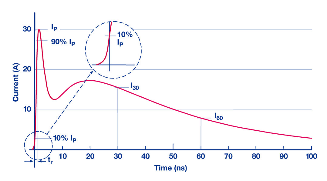
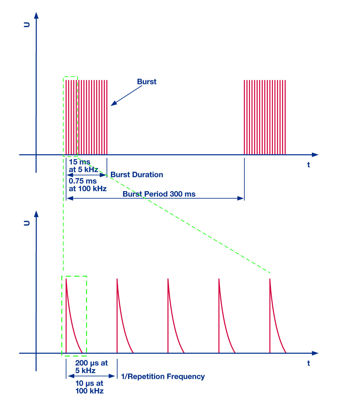
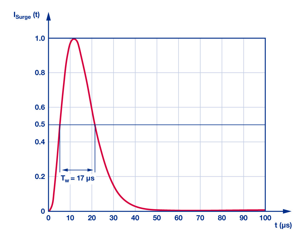
These products have only been tested under the ESD standards. EFT is unique in that the strikes hit in bursts (5 kHz or more) and with a slower rise time (5 ns) although the voltages are not as high (4 kV and below). Surge has about 1000 times the energy per strike as EFT, but is 1/1000th as fast as waveform. If you need to cover these standards as well, make sure the protection components state that they can handle it on their data sheets.
Circuit protection in a nutshell
While an RC filter or a TVS diode seem like it is simple to toss in a circuit as an afterthought, remember all the other things mentioned in this article that will affect system performance and the protection level. This includes layout, the parts used on the front end, and the IEC standard that needs to be satisfied. If you keep this in mind early on, it may mitigate an emergency redesign during the final phase of your system design.
This article is far from a thorough overview. The topic of sensitivity will receive a deeper treatment in our follow-up articles. Additionally, other challenges in base station receiver design include automatic gain control (AGC) algorithms, channel estimation, and equalization algorithms. We plan to follow this article with a series of technical articles with the aim of simplifying your design process and improving your receiver system understanding.
References
The author thanks the International Electrotechnical Commission (IEC) for permission to reproduce information from its international standards. All such extracts are copyright of IEC, Geneva, Switzerland. All rights reserved. Further information on the IEC is available from iec.ch. IEC has no responsibility for the placement and context in which the extracts and contents are reproduced by the author, nor is IEC in any way responsible for the other content or accuracy therein.
IEC 61000-4-2 ed.2.0
Copyright © 2008 IEC Geneva, Switzerland. www.iec.ch
IEC 61000-4-4 ed.3.0
Copyright © 2012 IEC Geneva, Switzerland. www.iec.ch
IEC 61000-4-5 ed.3.1
Copyright © 2017 IEC Geneva, Switzerland. www.iec.ch
About the Author
Tony has a B.S. in electrical engineering, as well as minors in computer engineering, physics, and mathematics from California State University, Chico. He has a background in industrial automation in a manufacturing environment. He supports precision amplifiers at Analog Devices and is an all-around fun-loving guy.


