
Using FPGAs to minimize power in high-speed, DSP-intensive system designs
May 01, 2015

Power reduction is increasingly important for high-speed, DSP-intensive system designs. For instance, in communications systems, communications must b...
Power reduction is increasingly important for high-speed, DSP-intensive system designs. For instance, in communications systems, communications must be enabled in periodic bursts, eliminating constant power usage in amplifiers and the rest of the system. In sensor networks, the requirement is to turn off active sensors periodically (i.e., for traffic images or weather sensors), or to turn them on (i.e., in the event of an earthquake), and upload information in a burst before returning the equipment to sleep mode. In medical monitoring equipment that typically has relatively low sampling rates, low-power features are needed to implement periodic operation as a means of minimizing power consumption the same holds true for handheld portable solutions.
For power-aware DSP-intensive system designs, not only must designers deliver the lowest static power, they also must focus on the lowest possible total power, especially at high frequencies and temperatures. Field programmable gate arrays (FPGAs) contribute to this goal through a comprehensive approach to minimizing power. This approach encompasses process technology, architecture and the design of configurable logic, as well as embedded features including SERDES, DDR2/3 and DSP blocks, and the inclusion of special power modes that further reduce consumption to a level that is even lower than that of static power. This article focuses on the evolution of FPGA technology to address DSP challenges for low power DSP-intensive system designs.
FPGA evolution
In the last two decades, many advanced CPUs and MCUs have architected various power-saving modes to address the power consumption challenges caused by higher frequencies and higher integration levels in DSP-intensive designs. Only the most advanced FPGAs have been architected to provide similar advanced low-power capabilities while supporting higher-frequency devices. And only recently have FPGAs become available that address the leakage problems of earlier SRAM-based solutions, while also providing access to low-power modes for additional power-saving capabilities.
In general, three power components play a major part in total power consumption as it relates to the FPGA power budget: static power, dynamic power, and inrush power. These three components must be managed effectively to achieve the lowest power consumption.
Managing these components requires an inherent low leakage current – an important attribute if FPGAs are to support the power requirements of DSP-intensive designs. Flash-based FPGA solutions offer an advantage here as compared to FPGAs that use SRAM cells, because flash-based FPGAs are built using a single transistor (rather than six), and both configuration and inrush (during power-up) power are zero. SRAM FPGAs power up in an un-configured state and need to complete the initial power-up and reset sequence. At first, the various configuration bits are in unknown states and need to initialize on every power cycle. Hence, a current surge is created that may generate a spike as high as several amperes for as long as a few hundred microseconds, which results in an in-rush of power (see Figure 1).
|
|
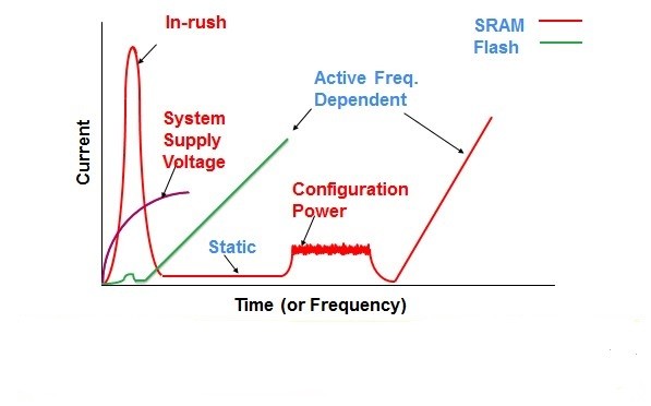
To mitigate this current spike, many SRAM FPGAs have added complex power-sequencing requirements to the system. Non-volatile flash-based FPGAs, on the other hand, do not need external configuration devices for reprogrammability, eliminating hundreds of milliwatts (mW) at device start-up and the need for external devices for mitigation. In some cases, a flash-based FPGA can deliver 1,000 times lower leakage per cell than an SRAM-based solution, along with the advantages of ultra-low static current and no requirement for external devices for mitigation.
In addition to the inherently lower power requirements of flash-based FPGAs, there are additional features that can be leveraged in order to further minimize power. Today’s flash-based FPGAs combine hard IP blocks and an FPGA on a single die, and integrate that FPGA with a full-featured microcontroller system, enhanced FPGA fabric and high-speed serial and memory interfaces. Additional power-conscious features and other capabilities include:
- SERDES enhancements: The latest FPGAs reduce power per Gbps for each SERDES lane to as low as 13mW, which can be up to five times lower when compared to other cost-optimized FPGA solutions with similar capabilities (see Figure 2).
- Integration of many different hard IP and other resources in smaller devices: By including more I/O, transceivers, PCI Express endpoints and a high-performance memory subsystem, it is possible to deliver more capabilities in smaller, lower-power devices.
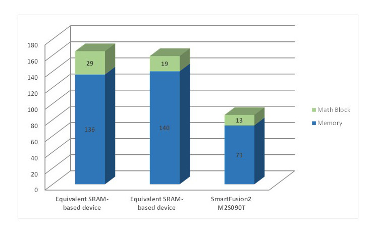
- Embedded RAM and math blocks: The flash FPGAs include the inbuilt hard RAM blocks and math blocks for intensive DSP applications. Also, these blocks deliver low power at high performance levels. Figure 3 shows the RAM power comparison between different FPGA manufacturers.
- Embedded processor subsystems with inherently lower power: Some subsystems offer multiple low-power modes including a sleep mode and a deep sleep mode. The use of low-power modes enables the rapid stopping and starting of the FPGA fabric and related I/Os, while preserving the state of the FPGA fabric and dramatically reducing power. It takes approximately 100 microseconds to enter the sleep mode and another roughly 100 microseconds to exit. While there, the state of the FPGA is maintained so that, upon exit, the device continues to operate from where it left off.
- The use of additional tools to minimize power: Users can further optimize their designs for lower power consumption by using various tools to compute power profiles and for smart floor-planning and power-optimized place and route.
|
|

|
|
All of these power-reduction features and capabilities are particularly important in high-speed, DSP-intensive system designs.
Challenges of DSP designs
DSP-intensive system designs require complex arithmetic computations, high memory bandwidth requirements, and high-speed serial transmission with dynamic reconfiguration. These requirements consume significant power at high performance levels. The new generation of FPGAs must be capable of handling these requirements with the lowest power consumption possible, and without compromising on performance. DSP system designers uses a number of different building blocks (multipliers, memories, transceivers, etc.) for their designs, and there can be significant differences in power consumption across various system architecture implementations depending on the FPGAs used.
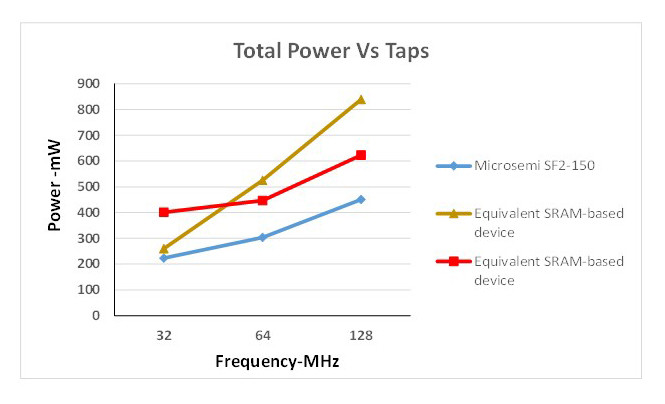
All FPGAs have hard multipliers as a basic computational unit and play a vital role in total power within the overall system power budget. To study this, Microsemi conducted research on finite impulse response (FIR) filters with different architectures and analyzed the power consumption of each based on the number of multipliers vs. the frequency of operation.
A FIR filter is a DSP block that is frequently used to remove unwanted noise while improving signal quality, or to shape signal spectrum in a variety applications. There are several FIR filter architectures, including transpose and systolic (with or without symmetry). Each of these two architectures has special characteristics related to total initial latency, the number of DSP blocks, the throughput or performance, and the number of pipeline registers. The difference between the two architectures is illustrated in Figure 4, which shows the symmetric versions of transpose and systolic 16-Tap FIRs.
|
|
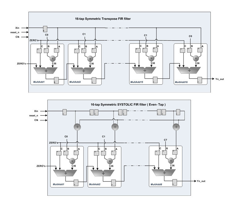
To summarize the differences between the two architectures, systolic architectures use pipeline stages and reduce the inputs fan-out to increase the frequency of operations; at the same time, though, the initial latency for N-Tap systolic FIR is (2*N -2)-cycles. In comparison, while transpose architectures run at a lower frequency, their initial latency is better (N-1 cycles) and they use fewer sequential resources. There are other issues to consider with these architectures. One of the most important is filter stability, especially when there are a large number of taps and weighting features must be taken into account. For instance, in a voice processing application where echo cancellation is required, the weights need to be higher at the near end where most of the echo exists, and lower on the later filter taps where there is less echo.
FPGA power consumption can vary dramatically depending on which architecture is used. In one study, power estimation tools were used and actual silicon measurements taken at various temperatures for FPGA development kits across 32-, 64- and 128-Tap Transpose FIR implementations. The study showed that, when properly designed and implemented, FPGAs deliver significant power savings. Additionally, these savings are even more pronounced at lower frequencies and high temperatures. Another important finding is that, for the best-performing FPGAs, power dissipation is linear to the number of Taps. In other words, power dissipation figures are worse for some poor-performing FPGAs when the number of Taps is low, while in others, they are worse when the number of Taps is high. This may be due to architectural issues.
|
|
Conclusion
Today’s DSP-centric system designs are under growing pressure to minimize power across a wide range of applications. By reducing total rather than just static power, today’s flash-based FPGA technology is playing a key role in enabling the next generation of high-speed, DSP-intensive system designs that must deliver high algorithmic performance in ever-shrinking form factors with the lowest possible power consumption.


