
Protect your Circuits from Electrostatic Discharge Damage
May 17, 2019
Blog

This type of damage is most apt to occur in the assembly process or before the chips have been assembled into their final PCB resting place.
Yes, theory is grand, but there is nothing like reality bringing you out of the clouds. With today's electronics, we supposedly have all ESD bases covered through the design of robust ESD structures in our integrated circuits. We think all is well and that our circuits are safe until we start working without a thought to ESD protection.
The definition of electrostatic discharge or ESD is the transfer of electrostatic charge between bodies or surfaces at different electrostatic potentials. This event occurs at high voltages in short durations, in the kilovoltage (kV) range from 1 to 100 nanoseconds (ns). As you can imagine, with these types of voltage and time units, ESD events have fast edges. When such an event occurs, there is a transfer of stored static charge and a visible or invisible spark occurs.
You can experience your own personal ESD event by walking across a carpet in your leather sole shoes and touching your companion on the nose. This is a shocking experience, at least for one of us, but not deadly. A palpable spark is easy for humans to identify; but it is the invisible sparks that are so small, only our electronics with sensitive interfaces can detect. It is very possible for an individual to unknowingly cause destructive ESD circuit damage by touching a device without ESD protection. I know this from a personal experience. In a heavily charged ESD environment, an ESD protected silicon chip inside its package will be destroyed (Figure 1).
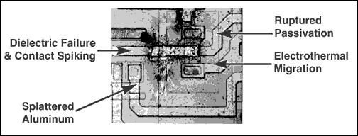
In Figure 1, the silicon has been exposed to an ESD event. The damage caused is catastrophic, with an evaporated metal trace, a compromised passivation region, and a possible electrothermal migration soft error. Technically, if the circuit is still operational, soft errors (a.k.a. specification degradation) may appear at a later date.
This type of damage is most apt to occur in the assembly process or before the chips have been assembled into their final PCB resting place. The internal ESD protection circuits of an IC offer some protection to the silicon during preassembly handling and assembly operations. In this environment, low-impedance ground paths serve as discharge paths. In the assembly or IC test environment, the implementation of low-impedance ground paths includes wrist straps, grounded floors, grounded desk tops, and ESD ionizers. Once the IC is installed in the PCB and interconnected to other components, this protected environment dramatically diminishes the likelihood of a volatile ESD path. With proper ESD control and prevention, there is a good chance that the internal ESD circuitry is never exercised.
People often produce ESD sparks as they interact with their surroundings. These harmful sparks can change the properties of a semiconductor device by degrading or destroying the silicon entirely. ESD events are a serious industrial problem causing an annual expense of billions of dollars in damages. Before you select your final products, it pays to follow good ESD prevention practices in your lab and check your product data sheets for ESD protection specifications. Join me in a few weeks where I will give you silicon ESD testing strategies.
References
Bonnie Baker is an electrical engineer who has written three analog design books, starting with A Baker’s Dozen: Real Analog Solutions for Digital Engineering (2005). In past roles, Burr-Brown, Microchip, Texas Instruments, and Maxim Integrated facilitated her involvement in analog design and analog systems for the last 30+ years. Bonnie holds a Masters of Science in Electrical Engineering from the University of Arizona (Tucson, AZ) and a bachelor’s degree in music education from Northern Arizona University (Flagstaff, AZ). In addition to her analog design fascination, Bonnie has a drive to share her knowledge and experience through the authorship of over 500 articles, design notes, and application notes.


