
Programmable perks: Tallying the benefits of FPGAs
March 01, 2012

Leaders in the field of FPGAs share their thoughts on how FPGA technology can simplify and add functionality to embedded designs.
|
|

ECD: With higher power requirements and recurring costs than custom logic or ASICs, which projects are best suited for FPGA technology?
BURICH: FPGAs have benefited significantly from Moore’s Law, and as a result have been able to stay at the bleeding edge of process technology while at the same time considerably reducing power consumption and development costs. As the costs of advanced process technologies rise (about $60 million for an ASIC at 40 nm), it gets harder to justify the upfront R&D costs. Today, we see a shrinking number of applications that can justify a leading-edge ASIC – mostly restricted to cell phones, PDAs, video games, and other high-volume applications. Those who can’t justify such an upfront investment seek to use trailing-edge process technologies.
In contrast, FPGAs can afford to use the latest process node and take advantage of Moore’s Law because there is a much wider array of applications that FPGAs can target. Today’s leading-edge FPGAs are 2-3 process nodes ahead of where most ASICs are, giving users the most advanced process technology available plus all the accompanying benefits at an overall lower cost. Development costs of leading-edge FPGAs are dramatically reduced because FPGA vendors can aggregate development costs across thousands of designs and customers. FPGAs are ideally suited for industrial, communications, automotive, military, medical, aerospace, and other designs with sub 1 million volumes or where a high degree of flexibility is required.
GETMAN: You have to be careful not to take an overly simplistic view when looking at power and cost and comparing different components like ASICs, ASSPs, FPGAs, and new hybrid products like Extensible Processing Platforms (EPPs). The comparison cannot just be at the device level; it also requires analysis at the system level and overall project level.
Design engineers must first answer some tough questions concerning costs, tool availability and effectiveness, production volume, time to market, and how best to present this information to management to gain support throughout the design process.
It’s interesting to compare these technologies, but in the end, the application is the final differentiator. A list of design objectives in order of importance, including cost (both development – nonrecurring engineering, and production – recurring unit cost), die size, time to market, tools, performance, and IP requirements must first be created. Then ask which technology best meets those objectives.
That analysis cannot just stay at the device level, where ASSPs and ASICs have an advantage with regard to both power and cost. For ASICs, the upfront cost means that only very high-volume applications can efficiently use an ASIC. Another trend is for companies to develop “kitchen sink ASICs,” where the design requirements for many different end products are the same, thus a single ASIC targeting multiple applications can be developed. However, this creates a problem with design complexity and project risks. Therefore, many customers are moving away from this approach after experiencing product delays and receiving products that, in the end, do not serve anyone’s needs perfectly. The other disadvantages that kitchen sink ASICs bring are that the silicon area is “inflated” to accommodate all the target applications, and therefore is less cost- and power-efficient.
We have always told our customers that if you have an ASSP that does exactly what you want and do not need or want to differentiate your product through hardware functions, then maybe that ASSP is the right choice for you. Most designs, however, can benefit from a flexible, programmable device that targets their unique applications and differentiates their products from the competition.
To accomplish that, many ASSP users add an FPGA next to their ASSP. While this offers a certain level of flexibility, it can also present some performance and power consumption challenges, stemming from the interface between the ASSP and the FPGA. This is why in the past few years, we have seen a push for fully integrated FPGA solutions, as well as FPGA vendors starting to offer hybrid solutions like an EPP (see Figure 2).
|
|

Over time, FPGAs have begun taking commonly used blocks such as DSP multipliers, small block RAM memories, and even high-speed serial I/O to offer the best balance of features and flexibility. The Zynq-7000 EPP family uses standard ASIC techniques to harden close to 11 million ASIC gates in the processing subsystem. This type of architecture swings the financial and technical bar around total cost of ownership, performance, and power radically away from traditional ASICs.
Massive parallel processing capabilities are another key benefit of FPGA technology, allowing designers to reach a level of performance not achievable with ASSP products. Additionally, using FPGAs within an EPP greatly reduces the risks involved when designing with ASICSs and ASSPs, as these devices cannot accommodate late design changes and do not provide the flexibility of infield upgrades. FPGAs offer the ultimate system integration platform to meet the growing need for programmable systems that cut development cycles, enable adoption to changing standards, and extend product lifetimes through field upgradability.
This segues perfectly to reducing time to market, a major advantage for any company’s product. FPGA technology allows our customers to move to market quickly, often in a matter of weeks, while drastically reducing their R&D costs. We offer design engineers a blank device that can be configured and reconfigured on-the-fly to implement any logic function that can be performed by an application-specific device. FPGA technology allows our customers to make changes to their designs very late in the design cycle. Even after the end product has been completed and shipped, they can extend its useful life by reprogramming the FPGA.
Innovations in FPGA technology have reduced the gap of power per device, making FPGAs much more competitive from a power standpoint. The battle to deliver maximum performance with minimum power expenditure is center stage in the evolution of the FPGA. Power conservation affects every budget, whether technological or financial. Product acceptability, reliability, and profitability depend as much or more on power efficiency as they do on performance, regardless of the type of project.
However, the key element of power savings will come from integration and reduced power consumption due to the chip-to-chip interface, which again, must be analyzed at the system level and not just at the chip level.
Increased system performance means new process technologies, massive parallel processing capability, advances in memory interfaces, high-speed transceivers (up to 28 Gbps), and no bottlenecks due to chip-to-chip interfaces. Decreasing power again relates to process technology, and in our case, this means using TSMC’s high-performance, low-power 28 nm process (a unified architecture across all of our 7 series FPGAs), other technology innovations, and burning no power to do chip-to-chip interfaces in a single device, as well as using fewer power supplies to reduce power consumption on the boards. Cost reduction is based on the use of a single device, which means there are no upfront costs and fewer components used on the board, resulting in a smaller bill of materials and a simpler design.
RILEY: The traditional trade-offs between FPGAs and ASICs/custom devices are still in effect. For a specific application, ASICs are lower power and lower cost, but they take much longer to develop and require a large upfront investment. What’s changing are the time-to-market requirements and useful market life for many projects.
Communications and wireless infrastructure developments are under tremendous pressure to get to market, driving engineers to consider process technologies that are reprogrammable and available today. In many cases, this is an FPGA. In the past few years, companies such as Lattice Semiconductor and SiliconBlue Technologies have been developing FPGAs that have solid capabilities and are priced well under $1. In fast-moving, cost-sensitive markets like consumer mobile, this type of solution is often the only way to add functionality in such a short time.
ECD: How can FPGA technology help embedded design teams deal with reduced budgets and increased system complexity?
GETMAN: While system complexity increases and the reduction of system design budgets becomes more of a reality, embedded system designers are jumping on the FPGA technology bandwagon to shorten design cycles, battle obsolescence, and simplify product updates. Using the constantly growing number of integrated FPGA development tools, reusable logic elements, and off-the-shelf modules, designers are creating new and innovative embedded systems that can be easily reconfigured for updates and changes in requirements with only a minimum impact on engineering and manufacturing.
FPGA designs combine multiple components into a single package that reduces component count, board size, and manufacturing complexity. Processors, memory, custom logic, and many of the peripherals in a typical embedded project are now in the FPGA. Today’s FPGA architecture has grown into billions of logic blocks (equivalent to gates), and with programmable interconnection flexibility designers can easily create hardware functions that exactly match the needs of a specific embedded application.
Drop-in IP cores from device vendors, third-party suppliers, and the open-source community ease FPGA set-up. The standardization of an IP interface (we use the AMBA 4 AXI standard) also greatly reduces design complexity when integrating functions into a single device. Furthermore, fueling a comprehensive ecosystem of hardware design tools, as well as software design tools and operating systems, is yet another key element of reducing design complexity.
Designers can segment FPGA-based signal processing algorithms into parallel computing structures to boost performance. High-level synthesis tools such as AutoESL can help simplify FPGA design and enable companies and developers not familiar with FPGAs or even hardware design to reap the inherent benefits of FPGA technology.
By utilizing a broad set of tools, the embedded designer’s tool bag for enabling FPGA technology has become increasingly mainstream. FPGA vendors are putting significant time and money into their development tools to improve the turnaround time, which will permit more iterations while reducing time to market and saving engineering efforts. The integration of many system elements into a single device reduces design complexity, as there are fewer chip-to-chip interfaces, as well as fewer performance bottlenecks.
RILEY: FPGAs are often used as bridging or coprocessing solutions. This allows embedded engineers to build systems out of the products they have. Can’t connect two dissimilar processors? No problem. FPGAs support a wide range of I/O types. Can’t handle the processing load? No problem. FPGAs can be configured to offload key functions.
FPGAs help get system products to market quickly, and the price and power of FPGA solutions has been dropping at a breakneck pace the past 10 years. FPGAs are used today in smart phones, tablets, laptops, handheld GPS devices, and many other platforms that were once the sole domain of custom logic.
BURICH: Designers today are challenged to get many different systems to market in shorter and shorter periods of time. By enabling easy customization for different features, price points, and evolving standards, FPGAs enable engineers to design a common platform and quickly spin off varying systems.
One of the most disruptive aspects of embedded design is adopting a new architecture to meet changing requirements. The industrial, medical, and military segments, for example, are also very concerned about product longevity and avoiding device obsolescence. By designing with FPGAs, customers can make incremental changes to a common design to adapt to changing market needs or industry specifications. Having a common tool flow with extensive design reuse addresses budget and time constraints.
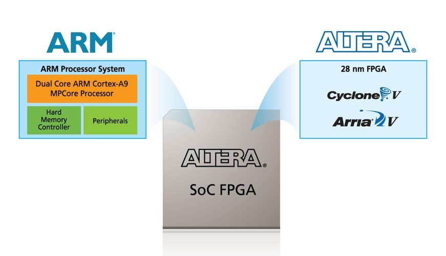
New System-on-Chip (SoC) FPGAs featuring hard ARM processor subsystems also help embedded design teams address reduced budgets (see Figure 3). Today’s leading-edge FPGAs are targeting 28 nm process technology, which relatively few commercial CPUs or ASSPs use. A monolithic SoC FPGA system maximizes power efficiency and software partitioning flexibility. SoC FPGAs allow hundreds of data signals to connect different functional areas, thus enabling 100 Gbps or greater bandwidth with nanosecond-level latencies, representing orders of magnitude better performance and latency than discrete implementations. Furthermore, monolithic integration permits memory controllers to be shared, allowing high-bandwidth memory access for hardware accelerators. A monolithic SoC FPGA implementation enables embedded design teams to increase system performance while lowering system costs and reducing power versus a two-chip solution.
|
|
ECD: One of the biggest obstacles to adopting FPGA technology has been the steep learning curve associated with development tools. How has this changed?
BURICH: This depends on the designer’s background. Those familiar with ASICs can quickly adapt to FPGA design flows and save time through the benefits of quicker verification in real silicon. Those who are not familiar with Real-Time Logic (RTL) will have a steeper learning curve. This is being addressed in two areas. The first is system-level design tools such as Altera’s Qsys, which enables designers to quickly assemble different design blocks using a higher-level graphic block environment. The second is automated RTL development from C language source. While this approach has been tried for many years, it is now coming of age for embedded developers with standards such as OpenCL. OpenCL also addresses the increasing challenge of designing multicore systems. Altera recently announced a program for evaluating FPGA-based OpenCL implementations.
GETMAN: Developing FPGA solutions can be complex, requiring the appropriate software tools. While each chip technology requires specific design tools, FPGA users are shielded from concerns of manufacturing yield and submicron issues by the nature of FPGA design flow, which brings ease-of-use, cost, and time-to-market benefits. FPGAs arrive fully tested and physically functional; the FPGA supplier handles physical design, verification, and characterization. Xilinx offers integrated design and debug tools for logic, DSP, and embedded processing, plus interfaces to third-party tools. FPGA design tools have improved dramatically, particularly [those] tools that apply high-level languages or interfaces to develop applications, such as MATLAB/Simulink from MathWorks.
Depending on the provider, software to program FPGAs varies in content and value-add features like compilation and editing tools. Very high-speed Hardware Description Language (VHDL) is the most common development language used. It allows FPGAs to be programmed via an easy-to-use graphical development environment. Additionally, FPGA vendors who provide tools such as development boards, support, and reference designs simplify the FPGA design process.
Conversely, there are longer design and verification cycles for ASICs, with a high likelihood of design re-spins and associated penalties. Plus, costly verification tools, training, and resources are required.
FPGA vendors who continue investing in software development tools and IP will enable more complex systems to be designed while carrying their silicon platform forward and promoting growth. The challenges going forward have not changed. These challenges continue to be reducing power, providing more capability at a lower cost, and further simplifying the programming. As progress is made on all of these fronts, the market share for FPGAs is increasing over ASIC/ASSP providers.
RILEY: The learning curve for FPGA design tools depends on where you are coming from. If you are an ASIC designer, the FPGA design tools will seem familiar. A design flow that includes HDL design entry, simulation, synthesis, and place and route is similar to an ASIC flow. For a software engineer who is used to programming in C/C++, the FPGA design flow will be new and require a learning curve.
Some vendors have claimed that you can write your code in C and their tools will automatically convert it to HDL. In my experience, this process still requires much human engineering to achieve the system throughput goal that drove the need to move beyond the confines of the microprocessor. There are well-established methodologies for partitioning a design between software and dedicated hardware. These still result in the best cost and performance, and FPGAs allow designers to experiment with different partitioning. Over the years, some FPGAs have included integrated processors, but they have not been successful. One reason for this is the lack of flexibility.
The world of microprocessors is vast. You can find any price, performance, or power point you desire from multiple vendors. Once you integrate the processor into the FPGA, your options become limited very quickly.
ECD: What types of IP core libraries do you offer to shorten the embedded design process?
RILEY: Lattice offers a wide range of IP cores, reference designs, and evaluation boards for PCI Express, Serial Rapid I/O, XAUI, Finite Impulse Response (FIR) filtering, Fast Fourier Transforms (FFTs), image and video scaling, MIPI interfaces, and more. Lattice focuses on the mid-range and low-density segments within the FPGA market. This means we concentrate on delivering high-end capabilities such as DDR3 memory interfaces and advanced filtering in low-cost, low-power FPGA platforms.
Lattice offers IP cores through a novel tool called IPExpress, which allows customers to change high-level parameters and generate new IP structures tuned to their feature, size, and performance requirements. Lattice provides many reference designs for free at our website. We also work closely with our customers to generate custom designs to meet their needs.
BURICH: IP libraries are important, and we offer a wide range of cores from memory controllers to embedded peripherals to high-speed communications interfaces. One of the most popular is our Video and Image Processing (VIP) Suite and our Nios II embedded processor IP. We also have a partner ecosystem that offers IP cores tailored to meet specific application requirements.
Just as important as the IP offering is the interconnect logic that ties the IP cores together into a coherent system. Altera offers a system integration tool (SOPC Builder) that automatically generates the logic that handles seemingly trivial yet critically important tasks of bus width adaptation, bus arbitration, bursting, interrupts, and more. We connect memory-mapped and streaming interfaces seamlessly and support high-performance bus standards like ARM AXI, as well as our lightweight, open Avalon interface standards. With the introduction of Qsys, we now generate a Network-on-Chip architecture offering even higher levels of performance and flexibility. Designers can not only assemble IP cores into a custom system, they can also create custom subsystems that can be shared internally to exploit the FPGA design reuse advantage.
GETMAN: Xilinx offers nearly 100 different embedded processing peripheral IP cores in categories including Processor IP Cores, Interface/Bus/Bridge IP, Peripheral IP, Communications IP, Infrastructure IP, Memory Controller IP, and Debug IP. These cores are included with the ISE Design Suite: Embedded Edition Development Kit and work directly in our Platform Studio, which supports MicroBlaze and PowerPC for PLB-based cores and MicroBlaze for AXI-based cores.
ECD: Which industry standards do you support to provide customers off-the-shelf, reconfigurable designs?
GETMAN: We see two aspects with regard to supporting industry standards, one at the external level and one at the internal level. At the external level, take the FPGA Mezzanine Card (FMC) defined in VITA 57 as an example. By using the reconfigurable I/O of FPGAs, design engineers can easily change a transceiver protocol or an I/O standard and route it through a different card connected to the FMC connector on our boards to create a new application/customer. Examples of internal standards that enable quick configuration/reconfiguration are AMBA 4 AXI, IP-XACT, and the proposed IEEE standard for IP Quality (QIP).
We support many interface standards for most market segments, including wireless communications, aerospace and defense, intelligent video, automotive, instrumentation, and medical imaging, which eases the connection to other systems. Having a comprehensive IP offering from Xilinx and its partners enables designers to quickly reconfigure their designs for applications or products.
RILEY: Lattice supports a wide range of hardware standards to help customers evaluate our silicon, design tools, and IP cores. Many of these evaluation boards are available for under $199, which allows customers of all sizes to experiment with Lattice products. Two standards that are popular with embedded designers are PCI Express and the Advanced Mezzanine Card. The AMC provides an FMC expansion connector, a USB-B connection to UART for runtime control, an RJ-45 interface to 10/100/1000 Ethernet, and an SFP transceiver module cage and connection.
BURICH: From the IP interconnect perspective, we support ARM’s AMBA AXI bus standard, as well as our own open Avalon bus standards (memory-mapped and streaming). Our Qsys system integration tool supports both AXI and Avalon, and the architecture of the tool is such that we can add other interconnect standards easily as needed.
From the IP interface standard perspective, we and our partners offer a wide range of IP cores that can be assembled into a custom system quickly with Qsys. Altera offers a wide variety of IP blocks of differing size and complexity, from the basic arithmetic blocks to transceivers, memory controllers, microprocessors, signal processing, and protocol interfaces. Altera and its third-party IP partners offer a broad portfolio of off-the-shelf, configurable IP cores optimized for Altera devices. Licensed and unlicensed IP is delivered and installed with our Quartus II design software.
ECD: Marketing materials for new processors with Advanced Vector Extensions (AVX) suggest replacing external FPGAs with code. Will this new architecture affect the FPGA industry?
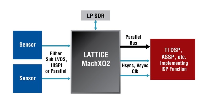
RILEY: AVX is an extension of the x86 instruction set targeted at improving performance, specifically in floating-point designs. Processors with AVX can work together with FPGAs to handle tasks such as bridging a dual-sensor interface to a new processor (see Figure 4). These extensions will allow embedded designers to do more with their x86 architectures; however, the performance gulf between a processor and an FPGA is still very large. Benchmark applications such as Finite Impulse Response (FIR) filtering, Fast Fourier Transforms (FFTs), and 2D image filtering are still many times faster on FPGAs than microprocessors. Also, FPGAs are superior for implementing general-purpose logic and bridging to dissimilar devices. So AVX will be a big help to many embedded designers, but it won’t obviate the need for FPGAs in embedded designs.
|
|
BURICH: Custom hardware has always outperformed software. The trade-offs of off-the-shelf hardware extensions are:
1. They might not be optimal for a broad range of applications; only custom, application-specific hardware can deliver the best performance. AVX offers benefits to the PC and tablet industries, but FPGAs already come with strong parallel processing capabilities and are the better fit for embedded markets. One-size-fits-all acceleration incurs the cost of answering a wide range of needs, resulting in inherent inefficiencies.
Off-the-shelf hardware extensions don’t lend themselves to establishing a competitive advantage because competitors have access to the very same hardware and software. Custom hardware can create a competitive differentiator and help developers create a product that outperforms the competition in both performance and revenue generation.
GETMAN: These types of specialized extensions are not new trends to the industry. As an example, MMX was introduced in the mid ’90s on Intel Pentium processors to improve multimedia processing. The ARM architecture is also enhanced with NEON extensions that serve a similar purpose.
In a design where an FPGA is used to perform simple accelerator functions for the main processor, the extra gain in performance from AVX will remove the need for some FPGAs. However, FPGAs are used for other functions beyond just simple accelerators, such as adding peripherals to the main processor, and the AVX architecture cannot address this need covered by FPGAs.
With the continual need for increased system performance, fixed defined instructions might not perfectly address a great deal of proprietary algorithm processing. This results in more clock cycles per function, yielding not only lower performance, but also higher power. This makes the massive parallel approach provided by FPGA architecture well-suited for hardware acceleration, thus enabling customers to continue achieving higher system performance. Therefore, the answer on industry effect is both yes and no.
In addition, FPGA companies have introduced new hybrid architectures (such as the Zynq-7000) that combine application-class processors and programmable logic. These new architectures offer the capability to add hardware accelerators in the programmable logic and have it controlled by the processor in a similar way as AVX. The massive parallel processing capabilities of programmable logic available in these hybrid devices enable performance beyond what AVX instructions could bring to a processor.
Altera
Linkedin: www.linkedin.com/company/altera
Facebook: www.fb.com/alteracorp
Twitter: @alteracorp
www.altera.com
Xilinx
Linkedin: www.linkedin.com/company/xilinx
Facebook: www.fb.com/XilinxInc
Twitter: @XilinxInc
www.xilinx.com
Lattice Semiconductor
Linkedin: www.linkedin.com/company/lattice-semiconductor
Facebook: www.fb.com/latticesemi
Twitter: @latticesemi
www.latticesemi.com


