
Microcontroller-based FPGAs hit the mark
November 11, 2015

FPGA vendors have been purposely pushing a growing divide in FPGA architectures. The main suppliers have gravitated to either SoC FPGAs with high-perf...
FPGA vendors have been purposely pushing a growing divide in FPGA architectures. The main suppliers have gravitated to either SoC FPGAs with high-performance application processors or offer low-end FPGAs with no processor. Applications such as server farms and high-performance computing require ever-growing increases in performance. To address this, many SoC FPGAs are incorporating ARM A-class application processors, which are well-suited for those applications. The reality for a multitude of other applications is that these processors are more than what is required. A-class SoC FPGAs are often too expensive, require too much software support burden because of the required operating system, and feature higher power consumption. Additionally, the raw compute performance is often not required.
On the other end of the spectrum, low-end FPGAs with no hard microcontroller or processor can be limiting for numerous designs. Low-end FPGAs only offer soft microcontrollers and there is no accompanying peripherals or subsystem. If peripherals are required then they must be created by using FPGA gates. Low-end FPGAs with a soft microcontroller run very slow, are inefficient due to the FPGA gates needed to create the microcontroller and subsystem, offer no security, and are developed on proprietary architectures.
For a broad class of applications, a hardened microcontroller-based SoC FPGA is often the more effective solution. A large amount of 32-bit microcontroller architectures are produced each year because there are numerous applications that can use them. Imagine if there was a microcontroller with a common subsystem of components and it also included a configurable block that could implement hardware acceleration tasks or other logic functions? An ARM Cortex-M3 SoC FPGA can be viewed as a microcontroller with configurable hardware acceleration. The hardware acceleration and implementation of logic functions are two key features where the FPGA fabric excels. Combined, an ARM Cortex-M3 and an FPGA fabric allow an ideal division of labor for many tasks in a wide variety of applications.
Partitioning design examples with processor and FPGA fabric
A microcontroller is ideal for slower-speed serial tasks because of the architecture and requirement to access memory for instructions. An FPGA fabric is ideal for parallel-processed functions that are more time critical. When partitioning a design in this manner, it becomes clear which functions each component should implement. For example, one of the main challenges of controlling multiple motors is the requirement for a deterministic response of the motor control loops. To ensure a reliable design, each motor must be serviced within a tight, deterministic time with no wide timing variation. Because the multi-axis motor control algorithm is a time-critical function, it should reside in the FPGA fabric. The FPGA is ideal to implement the control loops with tight deterministic timing. Figure 1 is a block diagram of a multi-axis motor control design. The bulk of the motor control algorithm is in the FPGA fabric, while the slower speed interfaces are connected to the ARM Cortex-M3.
|
|

The motor control algorithm is not the only required function. Often one or more communications interface and control I/Os are required for a complete motor control design. These interfaces are not high-performance oriented and are ideal for a microcontroller such as the Cortex-M3 to implement. The communication interfaces could be CAN bus, SPI, UART, or other control buses.
Adding data security to a design
The addition of data security requires a certificate and key exchange, as well as implementing encryption and decryption algorithms on the data. There are multiple data security handshake exchanges and support for multiple formats is often required. The exchange handshake is typically not time-critical, but each exchange algorithm has different strings that need to be parsed, various verification protocols, and multiple rounds of certificate checking. With all of these procedures and the lack of time criticality, it is ideal to implement the certificate and key exchange in a microcontroller such as a Cortex-M3. The appropriate code can be called and executed depending on the handshake exchange requested. Once the keys are exchanged and both devices are trusted, the data communication will need to be encrypted and decrypted. There are many wired and wireless communication speeds and protocols, and, depending on the link speed, performance is usually needed for the data encryption and decryption. When performance throughput is needed, it is recommended to implement it in the FPGA fabric. The transmitting device would implement an encryption algorithm such as AES 256, triple DES, RSA, or similar, and the receiving device would implement the same decryption algorithm. If the data link performance is not critical, the Cortex-M3 could implement the encryption and decryption. However, the FPGA fabric is ideally suited when higher throughput is needed.
Adding custom peripherals to a design
Although processors and microcontrollers offer common peripherals, numerous designs require custom interfaces. Many medical, industrial, and embedded designs often need to add additional interfaces, and open bus interface connectors address this issue. Two of the more popular peripheral bus connectors are the peripheral module (Pmod) and the Arduino shield. There are many peripheral designs that leverage these connectors and a SoC FPGA is ideal to bridge between these custom peripherals and the rest of the design. A microcontroller-based SoC FPGA can be uniquely leveraged when additional peripherals are required. The combination of the microcontroller and the FPGA fabric can implement bridging, acceleration functions, communication protocol management, I/O expansion, and control logic. One example is a design that needs to add a custom display. To interface to the display will require interface control logic, image manipulation and also register configurations. The ARM Cortex-M3 can address the latter and do other housekeeping tasks, while the FPGA is best suited for interfacing to the display and modifying the image as necessary.
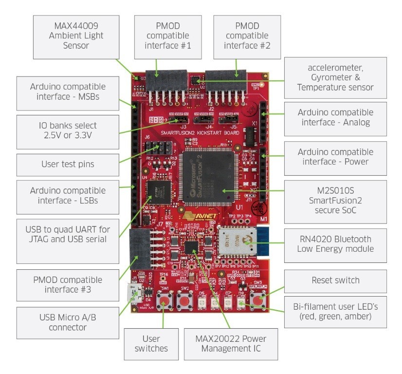
Avnet Electronics recently created a hardware kit to demonstrate the power that a microcontroller-based SoC can bring to the broad market (Figure 2). A number of peripheral options can be used with this board because it has both Pmod connectors and an Arduino shield connector set. Other key features include onboard peripherals, Bluetooth Low Energy (BLE), USB, and a host of sensors and switches. The board features the Microsemi SmartFusion2 SoC FPGA, which includes a hard ARM Cortex-M3 microcontroller and comprehensive subsystem. An HDL and C-code reference design, Windows-based software GUI, and Android app are included with the architecture for added flexibility. The Windows GUI can interface to all of the onboard components, and the reference design examples enable the ability to add on an Arduino shield or Pmod peripherals. When connecting to an Android phone using the Windows GUI, a full data security demonstration can be seen. This data security design implements the key exchange as well as encrypting the data between the SmartFusion2 FPGA and an Android smartphone.
|
|
There are a wide variety of general purpose applications that are ideally implemented in a microcontroller-based SoC FPGA that enables solutions such as bridging, I/O expansion, hardware acceleration, protocol management, and board initialization to be addressed. Using a hardware solution with a reference design and a software GUI allows design ideas to quickly become reality.


