
G-class amplifier cuts power when driving LCDs and OLEDs
April 01, 2015

The number of panes is growing rapidly, with no slowdown in sight. Hence, reducing their power consumption offers big benefits. LCD and OLED panels ar...
The number of panes is growing rapidly, with no slowdown in sight. Hence, reducing their power consumption offers big benefits.
LCD and OLED panels are the primary technologies for TV, computer monitor, or tablet displays. As the prevalence of these panels expand, it becomes more imperative to reduce their power dissipation and the junction temperature of the amplifier that supplies the backplane common node voltage (VCOM).
Both LCD and OLED technologies use a thin-film transistor (TFT) backplane to control each pixel by turning on and off individual TFT devices. A gate voltage is applied simultaneously to a specific panel row to allow the source voltage to flow to each pixel. Varying the pixel capacitor voltage controls each pixel’s light transparency and the overall display image. These TFT circuits are deposited using an Indium Tin Oxide (ITO) electrode, which is a semi-transparent metal layer. Because these transistor arrays are deposited by thin film deposition techniques, the quality of these transistors as switches is far from ideal.
A simplified electrical diagram of a pixel addressing circuit is shown in Figure 1. Each LCD pixel, represented by an equivalent capacitor (C), is connected to the source voltage whenever the gate voltage goes high and turns on the TFT. The source voltage value depends on the panel size, ranging from 0 V to 24 V for a 30″ to 70″ LCD panel, and 0 V to 8 V for a tablet-sized panel. The bottom terminals of all pixels are connected as the common backplane node voltage, referred to as common voltage, or VCOM. The VCOM voltage should be regulated and maintained as a single potential voltage across the entire panel area. To prolong the life of a panel and reduce image flicker, VCOM is typically set to a value slightly below the mid-point between zero and the maximum source voltage level.
 |
Manufacturing variation of the TFT backplane may result in significant variation in the VCOM voltage level from panel to panel, even in the same production line. As a result, the last quality inspection test of a panel module assembly adjusts the VCOM level and factory calibration setting for the optimum VCOM voltage for each panel. It’s also important to maintain a uniform VCOM level across the panel under transient conditions as the pixel information changes. To maintain the factory voltage setting, 1 to 12 channels of op amps, often called VCOM buffers, are linked to the DAC output of a digital potentiometer that contains the factory VCOM setting. Figure 2 shows a typical block diagram of a digital potentiometer and a single VCOM buffer.
 |
Modeling the VCOM buffers
In Figure 1, the capacitor representing each pixel can be modeled as a non-polarized capacitor. By doing so, the voltage polarity across each pixel doesn’t affect its brightness as long as the absolute value of the voltage remains constant. The image is not adversely affected by the periodic inversion of the polarity across the pixel capacitor.
Current flowing from the common plane to recharge the capacitor must be sourced or sunk by a VCOM amplifier. The peak-to-peak current transient depends on the brightness of each pixel and image characteristics.
To understand the electrical analysis of the VCOM amplifier’s behavior, the simplified model shown in Figure 3 can be used. In this model, an LCD panel is represented by a distributed RC load, and a square-wave driver represents a varying charge applied to the pixel capacitors. When a transient occurs, the VCOM output acts to compensate the change and to restore the original voltage across the common plain. The output voltage must settle before the end of the horizontal period, thus defining the VCOM amplifier’s slew rate and bandwidth requirements.
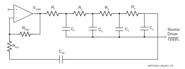 |
The VCOM amplifier has two feedback networks. A local DC feedback (RFB2) configures the amplifier as a follower. An additional remote AC feedback (RFB1, CFB) connects the middle of the LCD common plane to the op amp’s negative input and serves to speed-up voltage recovery of the VCOM plane.
Traditional VCOM buffer design
A VCOM amplifier is traditionally powered from a single analog power source called AVDD, whose specific value depends on the panel size and manufacturer. For a tablet-sized panel, AVDD can be 8 V with a VCOM target voltage of 3 V. During transient events, high peak currents flow from AVDD to the common plane and back from the plane to ground. The amplifier’s total power dissipation will depend on the peak current and VCOM output voltage.
The model simulation results in Figure 4 illustrate VCOM varying with the panel’s horizontal frequency and the amplifier’s output current. The results are image dependent; however, for all images, the transient nature of the load causes the amplifier’s power dissipation to increase, lowers its overall efficiency, and increases its junction temperature.
 |
GVCOM amplifiers provide stability and power savings
A G-class amplifier may be used to address the losses associated with traditional VCOM amps. G-class amplifiers utilize multiple supply rails (AVDD, VP, VN, and GND) to drive the amp’s output stage. A VCOM buffer would require two separate output stages connected to four voltage levels. For the tablet panel example using an 8 V AVDD voltage, VP can be selected as the tablet’s lithium-ion battery (nominally 3.7 V) and VN can be selected as the 1.2 V core voltage of the tablet’s digital ICs.
An example of a GVCOM buffer implementation is shown in Figure 5. Each output stage has a MOSFET connected to the amplifier output through a switch, labeled SW1 through SW4. The circuit also includes output-detect comparators to provide real-time comparison of the output voltage level and all supply rails. When the VCOM output voltage falls below VP, SW1 is turned off and SW2 is turned on, powering the output stage from the lower VP voltage. Under transient load, when the VCOM output rises above the VP rail, switches SW1 and SW2 reverse their position and the output current is delivered from the higher AVDD voltage.
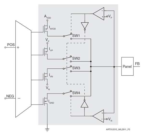 |
Similarly, the output stage selection also occurs when the op amp is sinking current. When the output voltage is above the VN rail, SW3 is turned on and SW4 is turned off. For a steady state 3 V VCOM output, the output stage is always powered between the VN and VP voltage rails, which significantly reduces the peak-to-peak voltage across the output stage and substantially decreases the amplifier’s power dissipation.
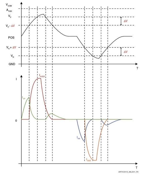
Figure 6 illustrates the amplifier’s output current flow during transient load. Initially, the output current is sourced by the VP voltage supply rail (green trace). As the output current increases, the second output stage turns on, which causes the output current to flow from the higher AVDD voltage (red trace). As the output settles back to its original value, the output current slowly transfers to the original output VP stage. The same process occurs when the output voltage drops to either VN voltage or ground. These results show how the total power dissipation in the amplifier is significantly reduced.
 |
Single-chip GVCOM amplifier solution
An example of a GVCOM implementation is shown in Figure 7. Exar’s iML2911 single-chip solution uses only the existing tablet power supplies (1.2 V, 3.7 V, and 7.6 V). The power input VP is connected to a lithium-ion battery with a nominal voltage of 3.7 V.
 |
The output power savings of an iML2911 GVCOM amplifier compared to a standard iML7831 VCOM amplifier in a tablet application is shown in the table. To account for the lithium-ion battery’s different voltage levels throughout its charge, the total power consumption was measured with VP voltages ranging from 3.0 V to 5.0 V. If VP was connected to a fixed power supply instead of a battery, this approach would also establish the optimal value for the VP supply rail.
Three different display patterns were tested: static, vertical, and sub-vertical. The static pattern is the standard tablet home screen; vertical and sub-vertical patterns are a sequence of black and while pixels. Although the vertical and sub-vertical patterns aren’t normally encountered, they’re commonly used in the industry to test LCD panels to estimate the worst-case thermal performance.
 |


