
Comprehensively Understand and Analyze Switching Regulator Noise
March 06, 2019
Story

This article will introduce several different types of inherent switching regulator noise: switching ripple, wideband noise, and high frequency spike.
Abstract
This article will introduce several different types of inherent switching regulator noise: switching ripple, wideband noise, and high frequency spike. The PSRRs of switching regulators as they relate to input noise suppression will also be discussed and analyzed. A comprehensive understanding of switching regulator noise is important when designing a low noise switching regulator in order to remove post-LDO regulators to improve power converter efficiency, save solution size, and lower design cost.
Introduction
Generally, traditional switching regulators were considered very noisy on output voltage compared to low dropout (LDO) regulator output; however, LDO voltage caused significant extra thermal issues and made the power design more complicated. Comprehensive recognition of switching regulator noise is necessary and can help when designing a low noise switching solution for the purpose of producing low noise performance at the same level as LDO regulators. A buck regulator with current-mode control was the analysis and evaluation objective since it was the most commonly adopted in application. Signal analysis was the primary method used to understand switching ripple noise, the present wideband noise characteristic, and where it comes from, and high frequency spike noise due to switching. The switching regulator PSRR (power supply rejection ratio) will be discussed, as well as the signal analysis method, which is important to input noise suppression.
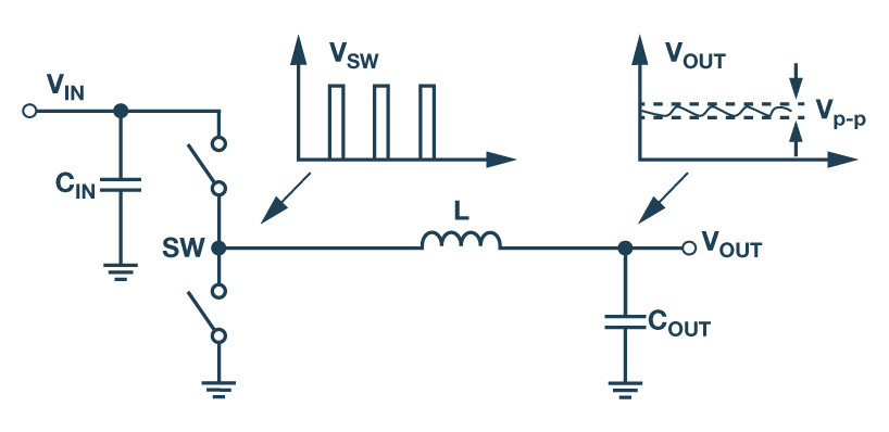
Switching Ripple Noise
This section presents the buck converter output ripple calculation formula in relation to fundamental and harmonic theory.
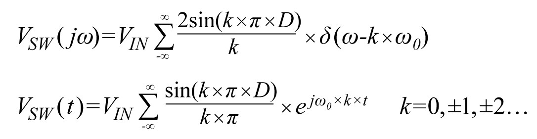
According to switching regulator topology and basic operation, the ripple is always the majority noise in a switching regulator, as the peak-to-peak voltage amplitude is generally several mV to tens of mV. It should be considered a periodic and predictable signal. It can be recognized and measured easily through oscillation scope in time domain or Fourier decomposition in frequency domain if it operates on a fixed switching frequency.
Where:
VIN is input voltage. D is duty cycle, which is equal to VOUT/VIN for buck regulator.
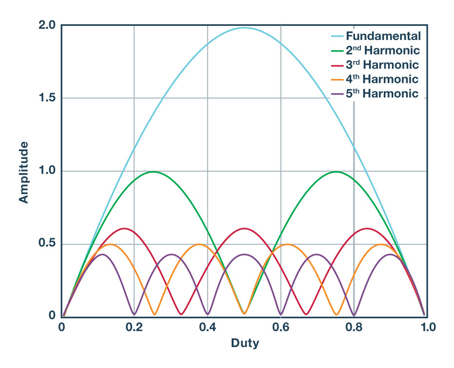
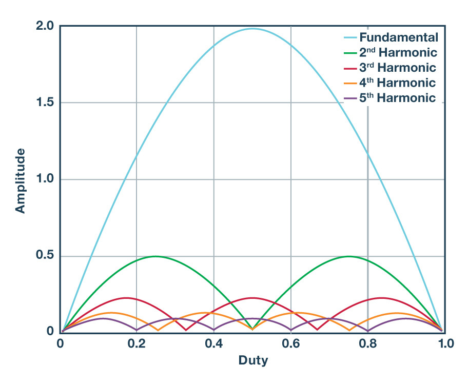
The VSW fundamental and harmonics component only depends on duty cycle when VIN is determined. Figure 2 shows the VSW fundamental and harmonic amplitudes in relation to the duty cycle. The fundamental dominates the ripple amplitude when the duty cycle is close to half.
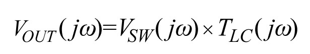
The buck regulator output LC stage transfer function is as follows:

Where L is the output inductor value, DCR is the inductor resistor value, and CL is the inductor parallel capacity value.
COUT is output capacity value. ESL is capacity series inductance. ESR is capacity series resistor value.
So the VOUT can be expressed as follows:
To simplify the calculation, we assume 20 dB per decade for the output LC stage, then the VOUT ripple fundamental and harmonic amplitudes in relation to the duty cycle, which are shown in Figure 3. The third, or odd, harmonic will be higher than an even harmonic when the duty cycle is close to half. Higher harmonics will have lower amplitude due to LC suppression and quite small proportions in comparison to the total ripple amplitude. Again, the fundamental amplitude is the majority component in the switching regulator output ripple.
For the buck regulator, the fundamental amplitude will relate to input voltage, duty cycle, switching frequency, and LC stage; however, all of these parameters will impact the application requirements like efficiency and solution size. To further reduce ripple, an additional post filter is recommended.
Wideband Noise
The wideband noise in a switching regulator is a random amplitude noise on the output voltage. It can be represented by noise density in
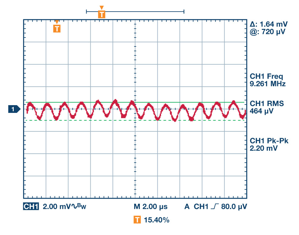
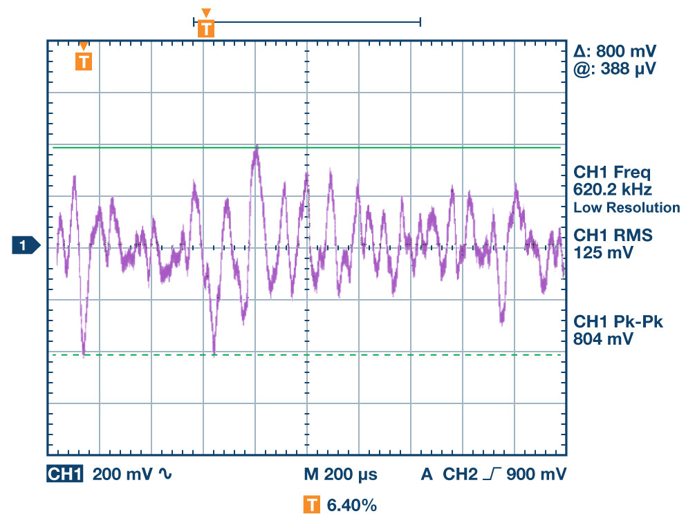
The typical buck regulator wideband noise peak-to-peak amplitude voltage is approximately 100 μV to 1000 μV, which is much less than switching ripple noise. If you use an additional filter to reduce switching ripple noise, then the wideband noise may become the primary noise in switching regulator output voltage. Figure 4 illustrates that the primary source of buck regulator output noise is a switching ripple when there is no additional filter. Figure 5 shows that the primary source of output noise when using an additional filter is wideband noise.
To recognize and analyze switching regulator output wideband noise, it is necessary to have regulator control scheme and block noise information. For example, Figure 6 is a typical current-mode buck regulator control scheme and block noise source injection.
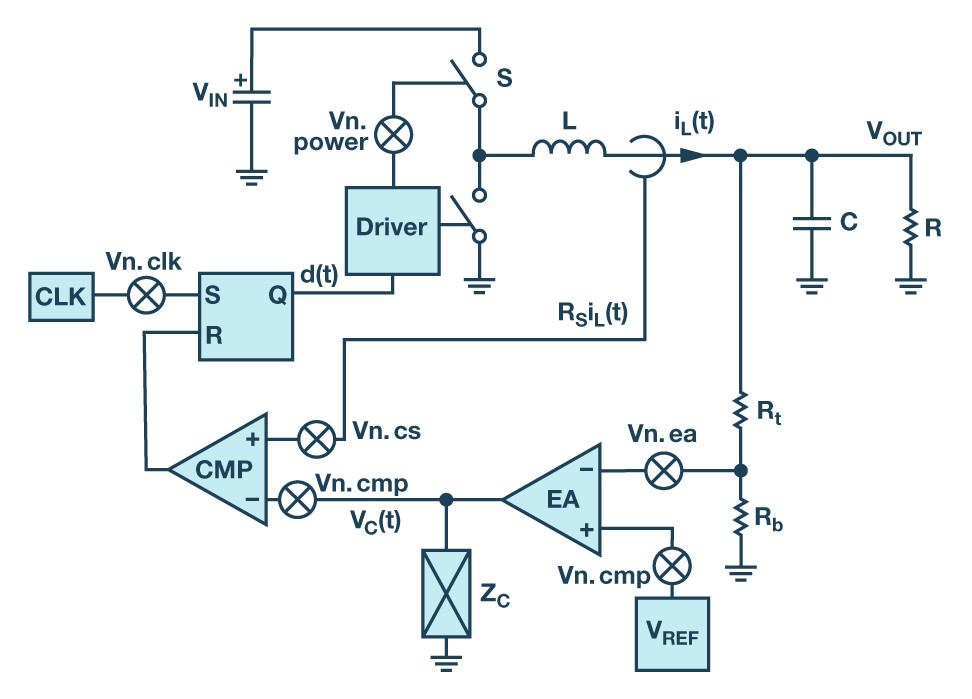
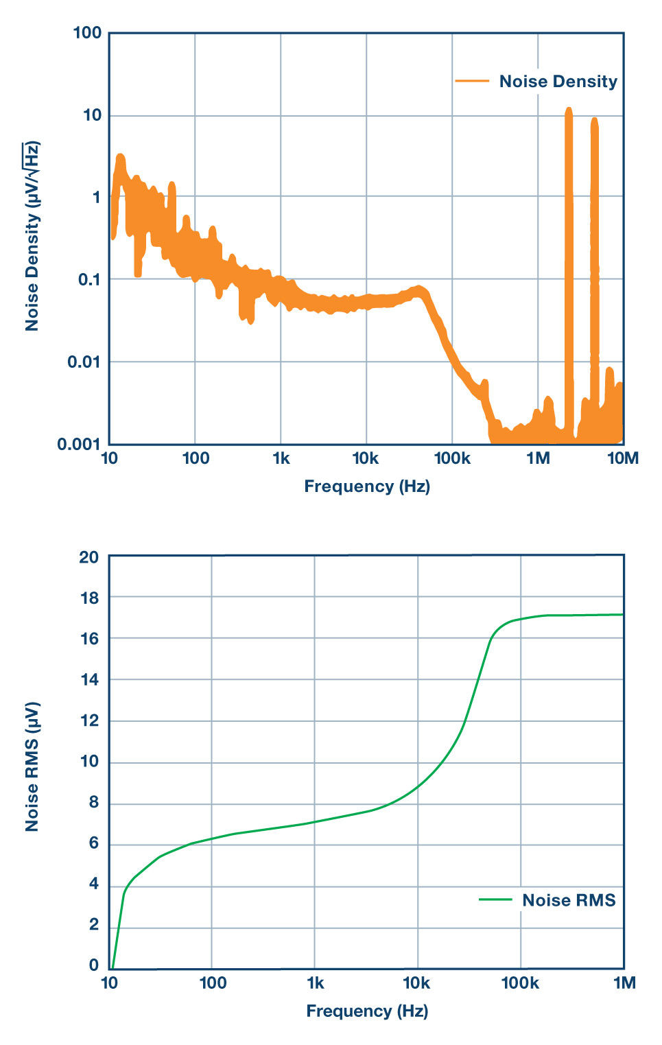
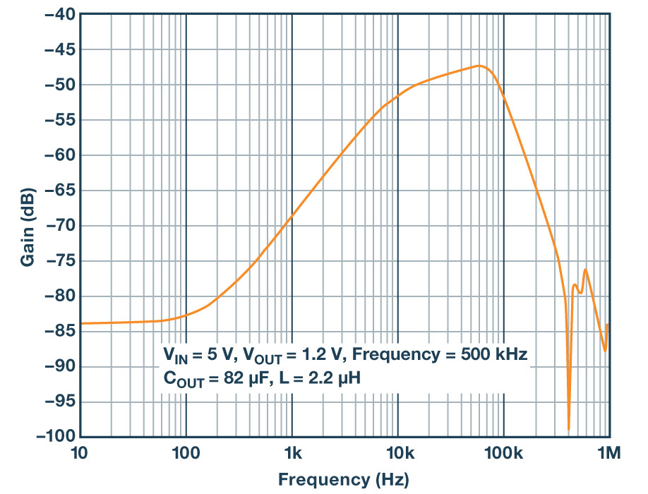
With acquired control loop transfer function and block noise characterization, there are two separate kinds of noise: loop input noise and inside loop noise. The loop input noise would transfer to the output within the control loop bandwidth, while noise is attenuated outside of the loop bandwidth. It is critical to design a low noise EA and reference for a switching regulator, as the unit feedback gain will keep the noise level, not increase it with the output voltage level. The biggest challenge is in digging out the biggest noise source within the whole system and reducing it in the circuit design. The ADP5014 is optimized for low noise technology with a current mode control scheme and one simple LC external filter, achieving less than 20 μV rms noise performance over the 10 Hz to 1 MHz frequency span. The ADP5014 output noise performance is shown in Figure 7.
High Frequency Spike and Ringing
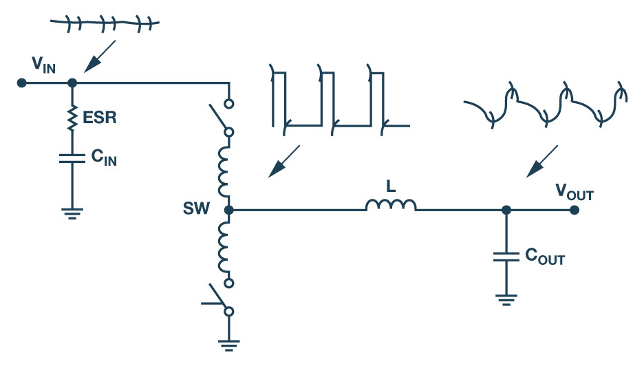
The third type of noise is high frequency spike and ringing noise as the output voltage is generated by the switcher turn-on or turn-off transient. Consider parasitic inductor and capacity in silicon circuits and PCB trace; fast current transient will cause very high frequency voltage spike and ringing at the SW node for a buck regulator. The spike and ringing noise will increase with higher current load. Figure 8 shows how the spike takes shape for buck regulators. Depending on the switcher turn-on/-off slew rate, the highest spike and ringing frequency would be within the 20 MHz to 300 MHz range, so the output LC filter may not be very effective at suppression due to its parasitic inductor and capacitor. Compared to all of the above talking about conductive path, the worst is radiation noise from the SW and VIN nodes, which will impact the output voltage and other analog circuits due to its very high frequency.
To reduce the high frequency spike and ringing noise, effective implementation of both application and silicon design is recommended. First, use an additional LC filter or bead on point of load. Usually this will make the spike noise on output much smaller than ripple noise, but this decision adds higher frequency components. Second, shield or keep away noise sources from the SW and input nodes from the output side and sensitive analog circuit, and shield the output inductor. Careful layout design and placement will be important. Third, optimize the switching regulator turn-on/-off slew rate and minimize the switcher’s parasitic inductance and resistance to effectively reduce SW node noise. The ADI Silent Switcher® technology also helps reduce VIN node noise via silicon design.
Switching Regulator PSRR
PSRR presents the switching regulator’s suppression capability from the input power supply noise to the output. This section analyzes the buck regulator PSRR performance at low frequency range. The very high frequency noise mostly impacts the output voltage through the radiation path instead of the conductive path as previously discussed.
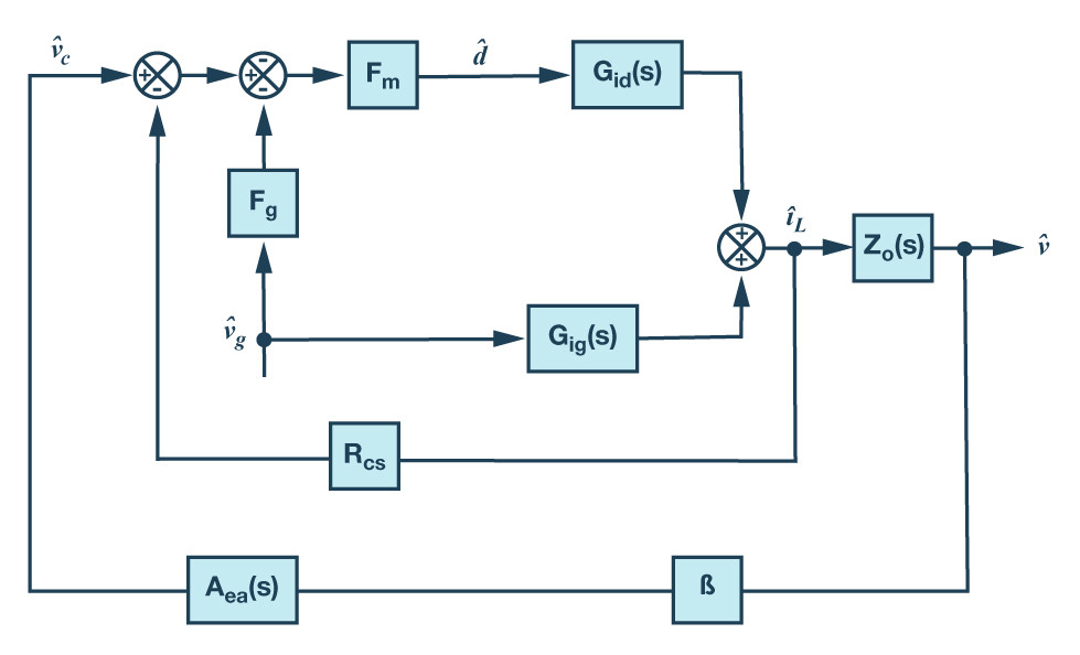
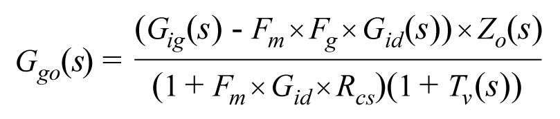
According to the buck small signal diagram in Figure 9, the buck PSRR can be expressed by
Where:
Fm is slope gain
Fg is input voltage to control
Rcs is current sense gain
Zo(s) is output cap and load
Tv(s) is loop transfer function

Compare the signal mode calculation with simulation results. The small signal mode is effective and matches the simulation results.
The switching regulator’s PSRR performance is dependent on the loop gain performance during low frequency range. Switching regulators have inherent LC filters that can suppress input noise in the middle frequency range (100 Hz to 10 MHz). That would be much better than LDO PSRR in those ranges. So, the switching regulator has perfect PSRR performance due to its high loop gain in low frequency, and inherent LC filters affect the middle frequency range.
Conclusion
More and more analog circuits, such as ADCs/DACs, clocks, and PLLs, require clean power supplies with high current. Each device will have different requirements and specifications for power supply noise in different frequency ranges. It is necessary to have a comprehensive understanding of the different switching regulator noise types and acknowledge the power supply noise requirement in order to design and implement an efficient and low noise switching regulator to meet the low noise specification of most analog circuit power supplies. Compared to LDO regulators, this low noise switching solution will have higher power efficiency, smaller solution size, and lower cost.
References
Morita, Glenn. “Noise-Reduction Network for Adjustable-Output Low-Dropout Regulators.” Analog Dialogue, Volume 48, 2014.
Morita, Glenn. AN-1120 Application Note: Noise Sources in Low-Dropout (LDO) Regulators. Analog Devices, Inc., 2011.
Felmlee, Matthew. AN-1066 Application Note: Power Supply Considerations for AD9523, AD9524, and AD9523-1 Low Noise Clocks. Analog Devices, Inc., 2017.
Reeder, Rob. Technical Article. “Designing Power Supplies for High Speed ADC.” Analog Devices, Inc., 2012.
About the Author
Leo Liu has worked at Analog Devices since 2005 when he joined the China Sales team as a field applications engineer. In 2011, he joined the Power Management Product Group as an applications engineer and has since been responsible for PMU product applications. He received B.S. and M.S. degrees in electrical engineering from Zhejiang University, Hangzhou, Zhejiang in 2001 and 2004. He can be reached at [email protected].


