
5 Special Registers That Have Transformed Today's SoCs
March 18, 2019
Story

In this article, we?ll cover five widely used special registers, namely; Alias, Shadow, Indirect, Lock, and Trigger-Buffer Registers.
In today’s SoCs, we have seen many innovations in the areas of system architecture, node-size, interconnect, security, programming language, and development tools. Sometimes we underestimate the significance and impact of the simple innovations that we use in our day-to-day work as SoC architects, verification engineers, hardware designers, or software/firmware developers.
In particular, let’s examine the innovations associated with the Hardware/Software Interface layer - where software applications communicate with the hardware peripherals. Specifically, in the register space where hardware peripherals such as Video Codec, Bluetooth or Wi-Fi receive the configuration, control and functionality from the software application executing on the processor. Ten years ago when designing registers, we only needed a combination of RO, WO, RW, RC, RS, WS, etc. But today’s SoC have become so complex that we have had to innovate and think of more creative ways to design registers. In this article, we’ll cover five widely used special registers, namely; Alias, Shadow, Indirect, Lock, and Trigger-Buffer Registers.
Alias Register
This is a type of register accessible from multiple addresses in the same address map, but physically it’s a single register. The fields in Alias registers have different behavior based on the address used to access them. As an example shown in Figure 1, fields in a RegA are readable and writable when accessed using 0x1000 address, but write-1-to-clear when accessed from 0x2000 address. Some guidance that should be applied when creating an Alias register: the hardware access of the Alias register is NA; a field cannot be an alias of an already aliased field; and the parent register of an aliased field cannot be external.

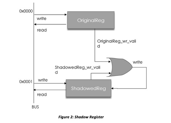
Shadow Register
When you have a software application that needs to overwrite all registers but the data needs to be restored later, the solution is to use a Shadow register. Data written to a register through the register bus shall be copied or shadowed to another register in the address map automatically. As shown in the example in Figure 2, the data in OriginalReg is copied to ShadowReg. The ShadowReg can be accessed from the bus, but does not have an effect on the Original register. Several shadow registers can shadow a single Original register.
Indirect Register
Some registers or memory locations are not directly accessible via a dedicated address, and they are called Indirectly addressed registers or simply Indirect registers. Two registers are used to access an Indirect register.
To store a value into the Indirect register array, a base register is employed to hold the actual address. The instruction inspects the base register, interprets its value as an address location in the register array, and places the value held in the data register into that location. To load a value from an Indirect register array, a base register is also employed. This base register holds the actual address. The instruction inspects the base register, interprets its value as the address, fetches the value stored at that location, and then loads it into a data register.
As shown in the example in Figure 3, Reg1 specifies the index into a memory array. Reg2 specifies the data to be written or stores the value that is read from the memory. Reg2 needs a “depth” property for the size of the Indirect register.

Lock Register
In the case of a state machine secured behind a register that can only be started by a key stored in another register, a Lock register can be the solution. Any writeable register or field can be protected/locked from writing depending on the value of field of some other register. Such registers are called Lock register. The Lock register and the protection/key register can be in different register groups but not in different blocks. As shown in the example in Figure 4, the Lock register specified by the property “lock” as defined by a simple expression lock=RegA.f1, which implies the register Lockreg is locked from writing depending on the value of the field “f1” of register “RegA,” the key register. The locking mechanism can also be defined by a more complex expression such as lock = regA.FldA || regB.Lock_fld == 8’b00000001 && regA.FldA == 4’b0011. This complex expression consists of different register fields. In this case, the software write access of register is locked if every condition within the lock expression evaluates to true at run-time.

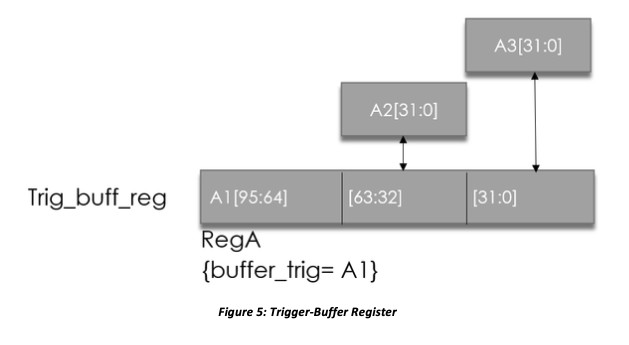
Trigger-Buffer Register
Sometimes it is required that a register with size greater than the bus width is written and read as one atomic unit from the hardware side. Such a register is written/read sequentially from the software side. This can be achieved by creating an N-register buffer in the memory space that is associated with a trigger event. When the trigger event occurs, the write/read happens to/from the buffer to the actual register that is available to the hardware side. The trigger event can be a read/write to either the Least Significant Bit or the Most Significant Bit register. As an example, shown in Figure 5, RegA is the wide hardware register, the MSB of wide register Reg.A1 is the trigger. Reg.A2 and Reg.A3 are the buffers corresponding to the fields of wide hardware register.
The next step is to learn how to define these special registers either in IP-XACT or SystemRDL. It is also necessary to learn how to code them in RTL and create the UVM register model and complete UVM testbench for verification. We cover the next steps in detail in our on-demand webinar, 5 Special Registers Useful for Today’s SoCs. In this webinar, we provide detailed information of these five special registers, their benefits, use cases, and examples. We also provide best-practices on how to automatically verify them where you can achieve 100 percent functional coverage.
Louie De Luna is Agnisys’ Chief Product Evangelist. He has over 15 years of experience in FPGAs, ASICs and EDA industries. He held various technical roles including design, applications, product management and marketing. He has practical experience in various verification methodologies such as simulation, CDC analysis, acceleration, emulation and prototyping. He received his B.S. in Computer Engineering from University of Nevada, Las Vegas in 2001.


