
Green up: Leading edge of 'green' mixed signal
February 01, 2010

This month, we explore examples of imec's basic research aiming to reduce power consumption to ultra-low levels in mixed-signal platforms.
This month, we explore examples of imec's basic research aiming to reduce power consumption to ultra-low levels in mixed-signal platforms.
A couple years ago we started hearing about how Moore’s Law was running into the laws of physics. To keep getting faster, digital circuits had to undergo some fundamental research and rethinking. With that, we’re seeing both the proliferation of asymmetric multicore and continuing progress on process, geometries, and materials that will keep things interesting for years to come.
Mixed-signal platforms are experiencing the same type of transformation. They’re driving things like data acquisition and wireless sensor networks and need to be battery-powered or driven from a harvesting scheme, thus falling into the ultra-low-power category.
The folks at imec, working with their research partners, are conducting some exciting studies looking at ways to reduce power consumption while still getting the necessary performance out of mixed-signal devices. Here are a few examples presented at this month’s International Solid State Circuit Conference.
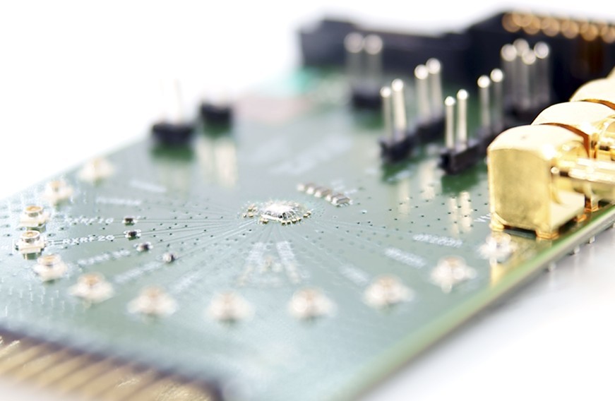
Heart activity signal processor
Packing an ECG readout channel, two quadrature readout channels for continuous-time monitoring of electrode-tissue impedance, and two quadrature readout channels for tracking signal fluctuations in a specific frequency band into 30 microwatts took some doing. This analog signal processor pictured in Figure 1 uses activity detection and adapts the sampling rate to match, saving power and reducing the tasks that the DSP and radio transmitter need to do.
|
|

Battery-less radios
A 2.4 GHz/915 MHz wake-up receiver in only 51 microwatts can be put in parallel with a conventional radio to wake it up only when necessary. The radio uses a double sampling architecture to overcome 1/f noise issues common at low data rates. The 90 nm implementation shows sensitivity of -75 dBm (SNR > 12 dB) for the 915 MHz receiver at 100 kbps on/off keying modulation. For the 2.4 GHz receiver, the sensitivity is -64 dBm and -69 dBm for 100 kbps and 10 kbps data rates, respectively.
Ultra-low-power ADC
Combining an asynchronous controller with successive approximation working completely in the charge domain, an 8-bit Analog-to-Digital Converter (ADC) consumes only 30 fJ per conversion step. The architecture avoids a clock-driven precharge phase, instead self-synchronizing to maximize speed and minimize power. The 90 nm CMOS chip consumes 69 microwatts at 10 MSps, with a standby power of 17 nW.
3GPP-LTE on a wireless transceiver
Working with Renesas and M4S, imec implemented a complete transceiver (RF, baseband, and data converter) compatible with a range of wireless standards in 40 nm low-power CMOS. The wireless transceiver shown in Figure 2 is fully configurable across all channels in bands ranging from 100 MHz to 6 GHz, with adaptable RF carrier frequency, channel bandwidth, noise figure, linearity, and filter characteristics. One of the primary targets for this device is 3GPP-LTE, but the reconfigurability idea is a drive to replace single-mode radios in many mobile devices.
|
|
These developments are probably the tip of the green mixed-signal iceberg that’s coming to a device near you in the near future. I’m excited to see this type of leading-edge research targeting key problems and paving the way for making all kinds of embedded devices greener.


